
Archive : 28 October 2008 year
New Holtek HT82K68A-L 1.8V Low Voltage Wireless Keyboard/Mouse Mask MCU
22:38In response to the needs of customers for low voltage Wireless Keyboard/Mouse microcontrollers, Holtek is pleased to announce the release of its new HT82K68A-L device. The device is an 8-bit MCU that includes 3K x 16 of Mask Program Memory, 160 x 8 of Data Memory, 34 bi-directional I/O pins, 3 high-drive function outputs, 8-bit timer, 16-bit timer, Low Voltage Reset function etc. In addition to these range of features, one special characteristic of the device is its ability to operate with a low working voltage of only 1.8V.
The HT82K68A-L is suitable for use in products where current consumption is an important consideration, among which are battery powered Wireless Keyboard/Mouse products. The low 1.8V operating voltage of this device is the lowest voltage among equivalent level products, taking a leading position among other competitor’s products. The HT82K68A-L is supplied in four package types, namely 20SOP, 28SOP, 32QFN and 48SSOP package forms, providing the customer with a choice according to their individual product application needs. As it is a Mask version device, it offers customers a high volume cost down device solution.

In full support of this new product, Holtek Semiconductor supplies a full suite of hardware and software tools. Known as HT-IDE3000, all the features one would expect from a high performance development system are provided. These include features such as real-time emulation, data memory and register reading and write functions, hardware breakpoints with logical setup, full trace analysis functions as well as many others. These combined features ensure that product designers have all the tools at hand to ensure the rapid and efficient debug and development of their new product applications.
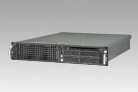
Fujitsu and Sun Unveil New Entry-level Server Powered by the SPARC64 Ⅶ Processor and the Solaris OS
22:15Fujitsu Limited and Sun Microsystems, Inc. today expanded their SPARC Enterprise® server family by adding the entry-level SPARC Enterprise M3000 server, powered by a single quad-core SPARC64™ Ⅶ processor and the Solaris™ 10 Operating System (OS). The SPARC Enterprise M3000 server inherits the mission-critical features of the SPARC64-based SPARC Enterprise server family, delivering mainframe-class reliability, availability and serviceability (RAS) in an ultra-dense open system at an entry-level price. The new systems are ideal platforms for single-threaded enterprise applications including databases, BIDW, ERP and CRM.
"The SPARC Enterprise M3000 server provides a perfect balance between mission-critical features, compact form factor and power efficiency," said Masami Yamamoto, corporate senior vice president of Fujitsu. "The new SPARC Enterprise server offers excellent performance for a broad range of application areas and will facilitate innovation in customers' business processes."
"Customers told us they wanted an entry-level SPARC Enterprise system, both for multi-tier application deployments and to create development environments for their larger M8000/M9000 systems," said John Fowler, executive vice president, Systems Group, Sun Microsystems. "The SPARC Enterprise M3000 server complements both the line and the mix-and-match reality of the datacenter. Customers now have a low-cost, high-performance option with mainframe-class RAS benefits in an open system running Solaris. It's mix-and-match or start small and grow big."
SPARC Enterprise M3000 Server Delivers Advanced Performance and RAS with the SPARC64 Ⅶ Processor
The SPARC Enterprise M3000 server leverages the same quad-core SPARC64 Ⅶ processor used in the world-record holding SPARC Enterprise M4000, M5000, M8000 and M9000 servers. With its Simultaneous Multi-Threading (SMT) chip architecture, the SPARC Enterprise M3000 server delivers excellent single-core performance. And with the latest I/O interfaces, PCI-Express, and SAS system architecture, the new system minimizes latency and provides maximum throughput, whether running compute, I/O, or memory intensive workloads. These new processors also help enable the SPARC Enterprise M3000 server to deliver double the performance while consuming over 50 percent less energy and space than previous UltraSPARC® Ⅲi-based servers.
The SPARC Enterprise M3000 server also delivers key features including hardware-level instruction retry, dynamic cache-memory degradation and extended ECC, giving customers the benefits of mainframe-like RAS capabilities at an entry-level price.
SPARC Enterprise M3000 Server Delivers Energy and Space Efficient Platform for Virtualization, Consolidation
At just two rack units (RU) weighing 22kg (49 pounds), the SPARC Enterprise M3000 server significantly reduces physical footprint and rackmount floor-loading, resulting in increased space efficiency. Leveraging Solaris™ Containers, the new SPARC Enterprise server provides an ultra-high density environment with exceptional virtualization capabilities and helps enable customers to optimally consolidate entry-level servers into a compact 2U chassis, letting them further reduce energy consumption and save space.
The SPARC Enterprise M3000 server also features two efficient cooling zones and an autonomous 9-stage fan control. This maximizes cooling and energy efficiency and minimizes noise: energy consumption is reduced by 50 percent or more over previous UltraSPARC Ⅲi-based servers and noise is reduced to 47dB, roughly the same noise level as a quiet office.
More information on the SPARC Enterprise M3000 server is available at:
http://www.fujitsu.com/sparcenterprise/ and http://www.sun.com/m3000.
Fujitsu and Sun Continue to Enhance the SPARC Enterprise Server Family
The SPARC Enterprise M3000 is the latest addition to SPARC Enterprise line of servers co-developed and marketed by Fujitsu and Sun. The companies are committed to building on their more than 20-year relationship through the continual enhancement of best-in-class products and services. Fujitsu and Sun plan to release systems based on new SPARC64 processors running at a clock speed of 2.8GHz in 2009. Fujitsu and Sun also have future enhancements planned for systems using the next generation of SPARC64 and UltraSPARC processors.
Product Availability and Services
The SPARC Enterprise M3000 server starts at $15,000 (U.S. List) and is immediately available directly from Fujitsu and Sun and their authorized resellers. Both Fujitsu-branded and Sun-branded SPARC Enterprise servers will be marketed worldwide. All features are identical.
Fujitsu and Sun also provide a full suite of services to help customers maximize their infrastructure investments. Services from both companies include consolidation, virtualization, maximizing data center efficiency and migration to Solaris 10. More information is available at http://www.fujitsu.com/ and http://www.sun.com/service.
From: http://www.fujitsu.com
Webcast Highlights Fundamentals of Motor Evolution
22:11Fairchild Semiconductor a leading global supplier of high performance products that enable energy-efficiency, announced the availability of a new webcast focusing on motor evolution.
With more than half of the world’s energy consumed in driving motors – such as air conditioners, refrigerators, elevators and factory automation – motor control is a prime application for energy-efficiency improvements. For example, moving from a single-phase AC motor to a variable speed motor can result in up to 40 percent energy savings.
The webcast discusses the need for electronic controls for motors, including power factor correction (PFC), energy-efficiency improvements and precision control of speed, torque and power.
The approximately 15 minute webcast examines the evolution of motors – from Faraday’s initial demonstration of the basic foundation of the electric motor through today’s developments in motor technology. The discussion includes the most common types of motors – Brush DC Motors, AC Induction Motors, Brushless DC Motors and Switched Reluctance Motors.
Fairchild is an industry leading supplier of high performance discrete and highly-integrated module solutions for motor applications. Fairchild’s power MOSFETs, Motion-SPM™ products, optocouplers, power switches, PFC-SPM™ products, HVICs, STEALTH™ diodes and triacs increase efficiency, simplify design and reduce system cost in motor applications.
For information on other products, design tools and sales contacts, please visit: www.fairchildsemi.com.Tektronix SignalVu Analyzes RF Signals Up to 20 GHz Bandwidth
22:06Tektronix, Inc., a leading worldwide provider of test, measurement and monitoring instrumentation, announced SignalVu™ vector signal analysis software for DPO7000 and DPO/DSA70000 digital oscilloscope series, enabling engineers to easily characterize and validate wideband and microwave spectral events.
One of the paramount trends in today's communications and radar systems is the need for increased information bandwidth and accurate phase and magnitude characterization of wideband signals. SignalVu combines the signal analysis engine of the RSA6100A real-time spectrum analyzer with the powerful triggering capabilities of the industry’s widest bandwidth DPO7000 and DPO/DSA70000 digital oscilloscope series, enabling designers to evaluate complex signals up to 20 GHz without a need for an external down converter. The unique combination provides the functionality of a vector signal analyzer, a spectrum analyzer, and the powerful Pinpoint™ trigger system capabilities of a Tektronix oscilloscope - fully integrated within a single RF test package at a lower price than alternative solutions. SignalVu advances productivity for engineers working on wideband RF components and system design, integration and performance verification, or operations engineers working in networks or spectrum management.
“The Tektronix SignalVu software rapidly displays RF characteristics in the frequency, time, phase, and power domains without the need for manual setups,” said Lynne Camp, vice president, Performance Plus Instruments, Tektronix. “The software works with the oscilloscope user interface to provide the best of both worlds: market-leading real-time bandwidth and triggers from the oscilloscope and a simple user interface for RF measurements. SignalVu running on DPO7000 and DPO/DSA70000 digital oscilloscopes provides engineers with improved time to insight while validating digital RF circuits and systems.”
Both terrestrial and satellite communications systems are driven by demands for greater and greater data rates, which drive bandwidth. Wideband signals have real-time or information bandwidth greater than 500 MHz and cannot be demodulated with traditional spectrum analyzers. Typical bandwidths for wideband signals range from 500 MHz to 4 GHz and carrier frequencies that extend well into the microwave region. Tektronix oscilloscopes provide real-time acquisition of signals up to 20 GHz. SignalVu vector signal analysis software shows time variant behavior of these signals, speeding design validation for applications such as wideband radar, high data rate satellite links, or frequency hopping communications.
“Engineers designing radar systems need to make a lot of standard pulse measurements on test waveforms,” said David Erisman, Chief Technology Officer, X-COM Systems. “Tektronix SignalVu can make 21 automated measurements on every pulse. This compares favorably to alternatives that offer only manual measurements, forcing users to locate and mark each pulse individually. Making traditional measurements readily available allows the engineer to verify the integrity of the data-set prior to post-processing. SignalVu running on a Tektronix scope will significantly improve ease of use and productivity for radar designers.”
Unique Integrated Functionality
Unlike alternatives, SignalVu software running on the Tektronix DPO7000 or DPO/DSA70000 oscilloscope hardware provides the integration of spectrum analyzer and digital oscilloscope functionality. Alternatives require operation in either oscilloscope mode or vector signal analyzer mode and attempting to mix modes will result in system errors.
SignalVu controls all scope acquisition parameters such as record length, vertical scaling and sample rate. SignalVu also makes effective use of memory; an acquisition is only limited by the amount of memory in the oscilloscope. For example, SignalVu software works seamlessly with the oscilloscope allowing users to utilize all of its powerful triggering capabilities. The ability to trigger on time and amplitude-varying events of interest is paramount in wideband system design, debug and validation. The Pinpoint trigger system within the DPO7000 and DPO/DSA70000 oscilloscopes allows selection of virtually all trigger types on both A and B trigger events whether they are transition, state, time or logic qualified triggers. Once triggered, SignalVu processes the acquisition for analysis in multiple domains.
Similarly, the Tektronix solution allows multiple measurements without a need to recapture the data. All signals in an acquisition bandwidth are recorded into the oscilloscope’s deep memory. Up to four channels can be captured simultaneously and each can be independently analyzed by SignalVu software.
Powerful Analysis
SignalVu vector signal analysis software utilizes the same analysis capabilities found in the RSA6100A series real-time spectrum analyzers. In addition to spectrum analysis, spectrograms display both frequency and amplitude changes over time. Time-correlated measurements can be made across the frequency, phase, amplitude, and modulation domains. This is ideal for signal analysis that includes frequency hopping, pulse characteristics, modulation switching, settling time, bandwidth changes, and intermittent signals.
SignalVu vector signal analysis software is now available for order on all DPO7000 and DPO/DSA70000 series oscilloscopes. The basic package is SignalVu Essentials that provides eleven core measurement and analysis capabilities. U.S. MSRP for SignalVu Essentials starts at $3,490 for the DPO7000 Series models and $4,990 for the DPO/DSA700000 Series models. Additional capabilities for pulse measurements and modulation analysis are available as options.
Atmel Announces Royalty Free NORTi's OS for its AVR32 UC3 32-bit Flash MCUs
11:03Atmel® Corporation announced today the availability of the popular uITRON 4.0 compliant NORTi operating system for its AT32UC3 32-bit Flash microcontrollers.
NORTi is a royalty-free operating system with a small memory footprint and a low performance overhead making it ideally suited for the powerful UC3 Flash microcontroller family. Being among the most popular operating systems in Japan and developed by MiSPO, NORTi includes uITRON 4.0 RTOS and a TCP/IP protocol stack and includes C source code. The offering includes support from our Japanese partner StepOne.
"The availability of uITRON-based NORTi RTOS is an important milestone in our launch of the AVR®32 UC3 flash microcontrollers in Japan," said Hirohiko Onishi, Japan Sales Director. "NORTi, in combination with the outstanding real-time performances of our AVR32 architecture, offers unprecedented value in the embedded market," he concluded.
"We have decided to port NORTi to the AVR32 UC3 architecture because we believe that it brings innovative features to the 32-bit market," said Hisanori Miyazaki, MiSPO President. "Customers reduce their cycle time resulting from the stable NORTi RTOS and as well NORTi facilitates the use of the software property of uITRON-based."
The AVR32 UC3 core is the first 32-bit microprocessor core in the industry to integrate single-cycle read/write SRAM with a direct interface to the pipeline that bypasses the system bus to achieve faster execution, better deterministic behavior and lower power consumption. The core today delivers up to 1.49 Dhrystone MIPS/MHz, running from on-chip flash memory. The AVR32 UC3 includes advanced features such as DSP arithmetic, single-cycle multiply and accumulate instructions and atomic bit or word read-modify-write instructions. The key benefits are high computational throughput, deterministic and real-time control, low power, low system cost, high reliability and ease of use. In addition, a peripheral DMA controller and multi-layer high speed bus architecture, makes UC3 core ideal for high throughput applications. UC3 devices are perfectly suited for portable and battery-based applications thanks to its outstanding performance/power consumption ratio up to 1.08 DMIPS per mW.
AT32UC3 microcontrollers rich feature set includes up to 512 KB Flash, up to 64 KB SRAM, Ethernet MAC, Full Speed USB with OTG, 10-bit ADC, SPIs, SSC, two-wire interface (I2C compatible), UARTs, general purpose timers, thirteen pulse width modulators and a full set of supervisory functions.
From: http://www.atmel.com
Atmel and Adeneo Announce Windows Embedded CE 6.0 Training on AT91SAM ARM9 Embedded MPUs
11:00Atmel® Corporation and Adeneo announced today a Microsoft® Windows® Embedded CE® 6.0 Training Course in Dallas, TX from November 17 to November 21, 2008. This event is an excellent opportunity for electronic system manufacturers intending to develop an application based on Windows Embedded CE and one of Atmel's powerful AT91SAM9 Embedded MPUs based on the ARM926EJ-S™ processor.
The goal of this training is to provide an in depth understanding of Windows Embedded CE internal mechanisms, and to present the technical information needed to start using Windows CE for designs. To make it practical and to give a better understanding of how Windows CE is implemented in hardware, the course is adapted to show examples on Atmel's AT91SAM ARM9-based microprocessor development platform.
As a special gift, Atmel offers to each attendee an AT91SAM9261 Evaluation Kit to continue their evaluation and development on Windows Embedded CE.
Adeneo has a proven track record as a Microsoft Embedded CE specialist for ARM-based Microprocessors, including Microsoft Gold Partner status since 2004 and the 2007 System Integrator Excellence Award from Microsoft. Adeneo is a Microsoft Windows Embedded Training Center since 2002 and the 2008 Training Partner Excellence Award from Microsoft. Atmel is a Silver Partner for Windows Embedded CE.
For further details, and to register for the course, visit: http://www.adeneo-embedded.com/srt/en/document/show?location.id:=1357&documentid=299 or contact sales@adeneo-embedded.com.
From: http://www.atmel.com
ANALOG DEVICES ENHANCES RF/IF SIGNAL CHAIN PERFORMANCE WITH HIGHLY INTEGRATED SYNTHESIZER AND MIXER FAMILY
10:57Analog Devices, Inc., a world leader in high-performance semiconductors for signal processing applications, today introduced the ADF4350 synthesizer with on-chip (VCO (voltage-controlled oscillator) and (PLL (phase-locked loop), which is the industry’s first fully integrated synthesizer to operate over an exceptionally wide continuous frequency range. Also today, ADI introduced a family of highly integrated active and passive mixers that are ideally suited for use in diversity communications applications. The active ADL5802 and passive ADL5356, ADL5358 and ADL5360 dual-channel diversity mixers expand ADI’s portfolio of main and diversity products and when coupled with the ADF4350 provide a highly integrated two-chip diversity down conversion solution for cellular base stations, satellite communications, and point-to-point microwave radio equipment.
The ADF4350 integrated synthesizer provides designers with a single, low phase-noise solution supporting a continuous tuning range from 137.5 MHz to 4.4 GHz. Alternative approaches require as many as 10 individual VCO/PLL combinations. The VCO in ADI’s new ultra-broadband, fully integrated synthesizer features phase-noise of –137 dBc/Hz at a 1-MHz offset when operating at 2.1 GHz, and –155 dBc/Hz at a 1-MHz offset when operating at 137.5 MHz. This corresponds to an integrated rms phase error of 0.36 degrees at 2.1 GHz and 0.02 degrees at 137.5 MHz. The ADF4350 provides two RF output ports and enables the user to digitally program the output power level.
Unlike competing synthesizers, the ADF4350 supports both integer-N and fractional-N operating modes, allowing the user to determine the optimal spur and phase-noise performance via software controls for optimal performance and faster time to market.
New Dual Mixer Family Addresses High Dynamic Range Applications
ADI’s new mixer family includes the ADL5802 wideband active device, which provides high linearity and modest gain in the industry’s smallest package footprint. The family also includes the ADL5356, ADL5358 and ADL5360 band-specific passive mixers, which achieve high linearity and a low-noise figure with integrated IF (intermediate frequency) amplifiers and offer higher gain compared to other active and competing passive devices.
The ADL5802 dual active mixer achieves an IIP3 (third-order input intercept point) of 27 dBm and a single sideband noise figure of 11 dB with a conversion power gain of 1.5 dB within a 4 mm × 4 mm LFCSP (lead-frame chip-scale package). For high linearity applications, the ADL5802 dissipates less than 1 W from a 5-V power supply. The ADL5802 uses high linearity doubly-balanced active mixer cores together with integrated LO (local oscillator) buffer amplifiers to provide high dynamic-range frequency conversion from 300 MHz to 6 GHz. A bias-adjust feature allows the input linearity, single sideband noise figure, and dc current to be optimized using a single control pin.
The ADL5356, ADL5358 and ADL5360 dual passive mixers with integrated IF amplifiers and integrated RF (radio frequency) balun achieve an IIP3 of 26 dBm, a single sideband noise figure of less than 10 dB, and an industry leading 10-dBm blocker noise figure of 16.5 dB. The passive mixers with IF amplifiers provide a conversion power gain of 8.5 dB to 9.5 dB within a small 6 mm x 6 mm LFCSP footprint. The 5-V (nominal) ADL5356, ADL5358, and ADL5360 can also be operated on a 3.3-V supply voltage for power-conscious applications.
The new active and passive mixers are well matched to ADI’s ADF4350 synthesizer. In addition, the ADF4350 provides an ideal LO source for Analog Devices’ ADL538X demodulators and ADL537x modulators. Together these products provide an ideal RF receive signal path when combined with Analog Devices’ AD837X family of high dynamic range variable gain amplifiers and Analog Devices’ ADL552X low-noise RF amplifiers.
Availability and Pricing
The ADF4350 is sampling now with full production scheduled for December 2008. The ADF4350 is available in a 5 mm × 5 mm, 32-LFCSP and is priced at $7.86 per unit in 5,000-unit quantities. For more information, visit http://www.analog.com/pr/ADF4350.
The ADL5802, ADL5356, ADL5358 and ADL5360 are sampling now and will be available in volume production in March 2009. The ADL5802 is available in a 24-lead LFCSP and is priced at $6.80 in 5,000-unit quantities. The ADL5356, ADL5358 and ADL5360 mixers are available in 36-lead LFCSP packages and are priced at $9.48 in 5,000-unit quantities. For more information visit http://www.analog.com/pr/ADL5802, http://www.analog.com/pr/ADL5356, http://www.analog.com/pr/ADL5358 or http://www.analog.com/pr/ADL5360.
From: http://www.analog.com
Atmel's picoPower 8/16-bit XMEGA MCU Cuts Power and Processing Requirement by 98%
10:55Atmel® Corporation announced its latest family of 32 MIPS, picoPower™ 8/16-bit microcontroller that radically improves MCU performance by off-loading interrupts and data transfers to an on-chip event manager and DMA. Atmel's AVR® XMEGA™ MCUs have several key benefits for the users:
- Highest performance with the AVR 8/16-bit single cycle core and FLASH program memory
- Reduced CPU active time with the new innovative XMEGA event system. With 8 routing channels to route direct communication between on-chip resources like ADC, Memory, I/O, timers and comparators the event system reduces the CPU active time by as much as 98%.
- Improved data rate, saved CPU load and reduced active time with the integrated 4-channel DMA controller. The DMA can transfer data between all memories and peripherals in any combination the users configure. The XMEGA DMA reduces CPU usage with 96% for SPI@4Mbps and 57% for UART@2Mbps.
- High speed and accurate sampling of analog data with two 12-bits, 8-channels and 2Ms/s ADCs. Integrated 64x gain stage increases the dynamic range to 18-bits.
- Market leading low power with Atmel's unique picoPower technology. Power down current is as low as 100nA and active current is cut up to 98%.
- Highest Flexibility with built in 5 different sleep modes, DES and CES crypto engines , WDT, USART, TWI, SPI, analog comparators, DACs, various 8/16 bits timers, EEPROM, SRAM, RTC, PLL and 6 different oscillators including a 1% RC oscillator and a 1uA 32kHz ultra low power oscillator.
Ingar Fredriksen, Atmel's director of AVR product marketing, explained, "We realized, after looking at a wide range of customer designs, that the majority of CPU cycles are spent handling interrupts and moving data. This realization meant that there was great potential to free up a significant amount of processing power by simply rethinking how various events are handled in the MCU. XMEGA microcontrollers are designed to revolutionize system performance, with lower power consumption."
100% pin- and code-compatible. All AVR XMEGA MCUs are pin- and 100% code-compatible across all devices. With XMEGA developers only need to keep and maintain one code base that can be used and re-used across multiple projects.
Availability and Pricing
Samples of the XMEGA devices are available now with flash memory density from 64 KB to 256 KB in 64 to 100 pin packages. Pricing varies from $1.75 to $5.00 depending on volume quantity and memory option.
NEWEST BLACKFIN® PROCESSORS EXPAND ANALOG DEVICES CONVERGENT-PROCESSOR PORTFOLIO, EXTEND LOW-POWER LEADERSHIP
10:51Analog Devices, Inc. (NYSE: ADI) unveiled the Blackfin® BF51x series, the newest members of the signal processing pioneer’s convergent-processor family. The new offerings continue to demonstrate the superior ability of the Blackfin convergent-processor architecture to reduce cost, power consumption, software complexity, and development schedules in a broad spectrum of mobile lifestyle, industrial and instrumentation, portable medical diagnostic and VoIP telephony applications. For additional information, please visit www.analog.com/BF51x . For the most up-to-date news, follow Blackfin at http://twitter.com/Blackfin.
The new Blackfin processors are the BF512, BF514, BF516 and BF518. All are single-core convergent processors that surpass outdated, heterogenous MCU+DSP approaches in reducing part-count, system cost, board space, and power consumption. Like traditional DSPs, the BF51x processors feature high clock rates and low power dissipation per unit of processing (MMACs/mW), and like traditional MCUs, these convergent processors are OS and compiler-friendly.
All four of the new 16-/32-bit BF51x processors are available at clock speeds up to 400 MHz (800 MMACS) and include 116 kBytes of RAM plus an optional 4 Mbits of serial (SPI) flash memory. Each also integrates Lockbox™ security for code and content protection. Owing to the needs of low power, rich media applications where Blackfin processors are best suited, on-chip integration assures easy connection to a variety of audio, video, imaging and communications peripherals and memory types. Integrated features include support for sixteen stereo I2S digital-audio channels, twelve peripheral DMA channels, and an advanced memory controller for glueless connection to multiple banks of external SDRAM, SRAM, Flash, or ROM. Each processor includes two dual-channel synchronous serial communication ports (SPORTs), a high-speed parallel peripheral interface (PPI), an I2C compatible two-wire interface (TWI), dual PC-compatible UARTs, and 2 SPI-compatible serial peripheral interface ports.
“System solutions ultimately determine how much power any particular application will consume,” said Jerry McGuire, vice president, General Purpose DSP, Analog Devices, Inc. “It’s quite intuitive that a single convergent processor with the right mix of integrated peripherals is always going to lead to lower BOM costs and power consumption than an inelegant combination of disparate processors and parts can possibly achieve. Many companies today talk about the lowest power or the highest performance. But what is important for today’s applications is the highest levels of performance at low power.”
Low Power Leadership – Performance at Low Power
All of the new Blackfin processors, delivering 8.5 MMACs/mW (100 MHz), include dynamic power management (DPM) functionality that lets developers match the processor’s power consumption to processing requirements during program execution. ADI pioneered the application of DPM more than seven years ago with the release of the first Blackfin processors –devices that have consistently maximized power efficiency since debuting in October 2001.
To maximize energy efficiency, while providing the highest levels of performance at low power, Blackfin processors use a wide range of advanced design techniques including programmable voltage and frequency scaling, clock-cycle resolution dynamic clock gating, multiple power domains that support deep-sleep and hibernate modes, high code density to minimize bus-activation energy, mixed threshold-voltage transistor utilization for optimal performance and power efficiency, a full-custom processor core for maximum energy efficiency, judicious use of hardware accelerators, and support for mSDRAM to minimize board-level power consumption.
| C550x | 18 mW | 60 MHz | ||
| Blackfin BF516 | 16.5 mW | 60 MHz | ||
| C550x | 46 mW | 100 MHz | ||
| Blackfin BF516 | 24 mW | 100 MHz |
Ideal for Portable, VoIP Telephony and Industrial Instrumentation Applications
The BF512 is the new low-cost entry point in the Blackfin processor family. The device balances performance, peripheral integration, and price, and is well suited for the most cost-sensitive applications including portable test equipment, embedded modems, biometrics, and consumer audio. All members of the BF51x family also include a new 3-phase PWM generation unit for inductive motor control applications and a quadrature interface for rotary encoders.
The BF514, BF516, and BF518 all extend the convergent processor family further into the portable application space with on-chip removable-storage interfaces. All three devices include Secure Digital Input Output (SDIO) for connectivity to standard flash memory and Wi-Fi cards; a power-optimized CE-ATA storage interface for small form-factor handheld and consumer electronics applications; and an embedded multimedia card (eMMC) interface for integrating mass-storage flash memory in a wide range of consumer electronics, wireless, navigation, and industrial applications.
For developers of network-connected industrial and instrumentation applications, the BF516 adds an Ethernet 10/100 MAC with Media Independent Interface (MII) and Reduced Media Independent Interface (RMII). Highly integrated for industrial, portable and VoIP applications, the BF518 Ethernet MAC supports the IEEE-1588 clock synchronization protocol for networked measurement and control systems.
An increasingly wide variety of applications are viewing the contemporary convergent-processor approach as the soundest choice for cost- and power-sensitive designs. For example, some voice-over-IP (VoIP) telephony system developers have designed in separate DSP and microcontroller chips to implement the required media and control functionality. With BF51x Blackfin processors, however, a single architecture enables full VoIP telephony functionality in a unified software development environment with faster system debugging and deployment, lower overall system cost, and the lowest possible system power demand.
“GIPS VoiceEngine media processing capabilities meet the highest requirements of VoIP equipment manufacturers and paired with Analog Devices' Blackfin processors we can assure customers a consistently high quality VoIP experience. The performance, power and functionality profile of Blackfin is a superb fit for VoIP technology,” said Larry Golob, Senior Director Business Development, Global IP Solutions.
With the Global IP Solutions (GIPS) VoiceEngine package of VoIP software components available for Blackfin processors, and a VoIP reference platform available on uClinux, the feature-rich Blackfin family has driven down the price required to easily design and deploy a fully scalable range of VoIP telephony designs across multiple market spaces.
Pricing and Availability
The BF51x family includes the BF512 at $4.95, the BF514 at $7.75, the BF516 at $8.75 and the BF518 at $11.85. Processors are sampling immediately. All prices are based on 25,000-unit quantities.
To view an Arrow Electronics, Inc. co-sponsored webcast on the new Blackfin family, please visit http://w.on24.com/clients/adi/BF51x.
From: http://www.analog.com
TI introduces the lowest power 1.8-V audio codec with integrated miniDSP in production today
10:46Texas Instruments Incorporated (TI) today introduced a highly integrated audio codec in full production with leading consumer electronics companies to help them meet growing consumer demand for cost-efficient, feature-rich products with better audio quality and longer battery life. The 1.8-V codec combines integrated power management and dual miniDSP audio processing engines to save designers total audio solution cost and make it easier to design advanced audio features in handsets, portable navigation and portable media devices. TI's PurePath™ Studio development toolset further eases design complexity and speeds time to market. And the codec's PowerTune™ technology increases playback time by allowing designers to tune the device for optimum power use in each operating mode.

"High-quality sound and feature-rich products are becoming an important consideration in portable product design, which traditionally has implied increased engineering investment to solve complex design issues," said Art George, senior vice president of TI's High-Performance Analog business unit. "TI is addressing these challenges with innovative products like the TLV320AIC3254. Customers are using the TLV320AIC2354 to differentiate their products with advanced audio effects, including multi-band equalization, dynamic bass boost, noise and echo cancellation. At the same time, they're reducing overall cost and complexity to speed their time to revenue."
miniDSP and algorithm library enhance audio performance and ease design complexity
The TLV320AIC3254 is the first product from TI to incorporate the highly programmable miniDSP audio processing engine, which allows users to run complex algorithms on the device while freeing MIPS on the primary processor. Leveraging TI's new codec and its 192-kHz sample rate, customers can add the most comprehensive suite of advanced digital signal processing capabilities to improve audio performance, including 20-band stereo graphic equalizer, multi-band dynamic range compression, custom FIR and IIR filtering, and 3-D processing, without in-house algorithm expertise or increased investment in resources for code development. TI will provide all low-level miniDSP programming. And designers can leverage the PurePath Studio development toolset and TI's library of advanced algorithms to compile, configure and load their application into the integrated miniDSP engines in an intuitive, drag-and-drop graphical environment, simplifying design complexity and reducing time to market.
PowerTune technology reduces power consumption to as little as 2.4 mW
The device also features PowerTune technology to extend battery life without sacrificing audio quality. This technology provides customers with the flexibility to optimize power consumption under any usage model, trading off between ultra low-power operation and signal-to-noise ratio (SNR) for better audio quality. For instance, designers concerned with power consumption can tune their system to consume as little as 2.4 mW in stereo playback when performance is programmed to the 90-dB SNR level. Conversely, customers seeking to maximize performance can achieve 100-dB SNR at 5.1 mW in stereo playback. To further increase performance, the TLV320AIC3254 also provides digital microphone support for improved system-level noise immunity.
Integrated power management simplifies design and reduces cost
The TLV320AIC3254 includes dual integrated LDOs, which provide additional power supply rejection and extend device capability to operate single-supply up to 3.6 V. With integrated stereo headphone amplifier, dual microphone programmable gain amplifiers, fractional PLL and analog input mux, the codec simplifies board design dramatically and reduces final system component count and cost.
Pricing and availability
The TLV320AIC3254 is available today in a space-saving 5 mm x 5 mm QFN-32 package from TI and its authorized distributors. The device is priced at $5.45 in 1000-piece quantities. Advanced audio algorithms are also available today.
In addition, for manufacturers seeking an ultra low-power audio codec without integrated miniDSP functionality, the pin-compatible TLV320AIC3204 is available for $3.45 in 1000-piece quantities. Samples, EVMs and software for both devices are available at www.ti.com/tlv320aic3254.
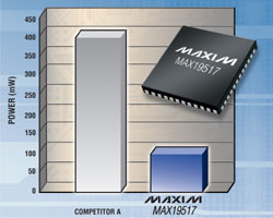
Industry's Lowest Power, Dual-Channel, 10-Bit ADCs Offer Superior Dynamic Performance
10:35Maxim Integrated Products introduces the MAX19515/MAX19516/MAX19517, a pin-compatible family of dual-channel, 10-bit, 65/100/130Msps ADCs. Offering the industry's lowest power consumption, the devices consume a mere 43mW (MAX19515), 57mW (MAX19516), and 75mW (MAX19517) of analog power per channel. Additionally, these ADCs achieve superior dynamic performance, with a 60dBFS signal-to-noise ratio (SNR) and 85dBC SFDR at 70MHz. Combining low power consumption with excellent dynamic performance, the MAX19515/MAX19516/MAX19517 are ideal for power-sensitive portable applications such as ultrasound and medical imaging, portable instrumentation, and low-power data-acquisition systems.
Designed for space-constrained applications, these ADCs integrate an extensive feature set to minimize the number of external components. They provide a self-sensing, analog supply regulator that allows the user to operate the parts from 1.8V, 2.5V, or 3.3V analog supplies. In addition, they feature single-ended or differential clock inputs; analog inputs with a wide, 0.4V to 1.4V input common-mode range to support AC- or DC-coupled inputs; and an on-board clock divider to eliminate the need for an external divider. Integrated CMOS output termination resistors allow users to program the CMOS output resistance, thus eliminating external damping resistors.
The MAX19515/MAX19516/MAX19517 are packaged in a 7mm x 7mm, 48-pin TQFN and are fully specified over the -40°C to +85°C extended temperature range. Prices start at $7.50 (1000-up, FOB USA).
National Instruments Expands High-Speed Digitizer Product Line
10:31National Instruments today announced the expansion of its digitizer product line with the introduction of three new digitizers/PC-based oscilloscopes. The 500 MHz NI PXI-5153 and NI PCI-5153 and the 1 GHz NI PCI-5154 modules round out the NI 515x series of digitizers, following the introduction of the NI PXI-5154 in July. With the NI 515x series, engineers can take advantage of a complete line of high-speed digitizers – with 300 MHz, 500 MHz and 1 GHz bandwidths – for demanding automated test and streaming applications where high-bandwidth measurements are required.
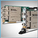
All three new products feature up to 256 MB of deep onboard memory per channel, providing accurate measurements by sustaining up to 2 GS/s real-time sampling rates over extended data capture windows. Engineers can use these digitizers to address a wide range of measurement needs in the consumer electronics, semiconductor, aerospace and defense and life sciences industries.
“High-bandwidth measurements are a complicated and expensive part of any automated test system,” said Ray Morgan, senior product engineer at ON Semiconductor. “With the 1 GHz PXI-5154 digitizer and the 2.7 GHz PXI-2547 8x1 high-frequency multiplexer, we created a low-cost 16-channel oscilloscope. The 1 GHz digitizer in the modular format has helped us test our new high-bandwidth products at a fraction of our previous test times.”
NI 515x digitizers are the first high-bandwidth digitizers on the market with three characteristics that make them optimized for automated test – tight synchronization between channels, ease of integration with other instrumentation and high data throughput. Using T-Clock technology, which synchronizes multiple instruments and was patented by National Instruments, engineers can integrate NI 515x digitizers with a variety of NI hardware, including arbitrary waveform generators and digital waveform generator/analyzers, to customize and build a complete, automated mixed-signal test system. Engineers also can synchronize multiple digitizers to build systems with up to 34 channels in a single PXI chassis, all simultaneously sampling at 1 GS/s and synchronized to picosecond-level accuracy between modules.
The PXI platform, upon which NI high-speed digitizers are built, provides measurement throughput up to 10 times faster than alternative instrument architectures because of the high-bandwidth and low-latency PCI bus. The digitizers’ high bandwidth, fast data throughput and tight multi-module synchronization are particularly beneficial for applications including mass spectrometry, radar, signal intelligence, non-destructive test and high-channel-count physics experimentation.
Engineers can combine the new digitizers with NI LabVIEW SignalExpress interactive measurement software to quickly acquire data, perform measurements and view and analyze data in Microsoft Excel or NI DIAdem test management software. Additionally, the NI 515x digitizers work with all National Instruments software including the NI LabVIEW graphical system design platform and the NI LabWindows™/CVI ANSI C development environment as well as other development environments such as ANSI C, Microsoft C++ and Visual Basic.
For more information on the new digitizers, readers may visit www.ni.com/digitizers/highspeed.
National Semiconductor Introduces Industry’s First Differential Wideband Amplifier with Programmable Output Limiting Clamp
10:25National Semiconductor Corp. October 22, 2008 introduced the industry’s first wideband 900 MHz fully differential amplifier to include a programmable output limiting clamp for protecting analog-to-digital converters (ADC) and other downstream circuitry from over-voltage events. The amplifier’s integrated clamp provides improved distortion, higher bandwidth and clamping accuracy compared with existing amplifiers that must use external discrete clamping circuits to provide the same protection.

The LMH6553 operates over the -40 degrees C to 125 degrees C temperature range and is well-suited for processing wide dynamic-range signals in automotive safety applications, including collision avoidance, lane departure and back-up warning systems. A member of National’s PowerWise® family of energy-efficient products, the LMH6553 features 900 MHz unity-gain bandwidth while operating on only 29 mA of supply current. This results in an industry-leading power-to-performance ratio of 32 uA per MHz.
Additionally, National provides designers with a variety of signal path solutions by pairing the LMH6553 with one of more than 40 differential input 8-bit to 14-bit ADCs featuring sampling rates up to 1 giga samples per second (GSPS). These ADCs include the ADC08D1000, ADC10080, ADC12C170 and ADC14DS105.
Key Features – LMH6553 Amplifier with Output Limiting Clamp
The LMH6553 operates across a wide supply range from single 4.5V up to a split +/- 6V supply. The LMH6553 provides 4 kV of electrostatic discharge (ESD) protection and its adjustable output clamp has a single reference control that sets the internal high and low clamp levels versus the multiple reference control levels required with external discrete clamps. Additionally, the LMH6553 features a 600 picosecond (ps) clamp overdrive recovery time and guaranteed +/- 53 mV clamp accuracy, allowing clamp levels to be accurately set relative to the desired signal.
The LMH6553’s -0.1 mV/degree C clamp-accuracy temperature coefficient provides excellent clamp level stability and enables signals to swing to within 22 mV of the clamp level before distortion degrades by 3 dB. The device’s current feedback architecture coupled with low input voltage noise of 1.2 nV/sqrt Hz and low input current noise of 13.6 pA/sqrt Hz delivers lower output noise at higher gain settings than other competitive differential amplifiers. The LMH6553’s external gain set resistors and the output common-mode control allow it to be configured for a variety of gains in AC- and DC-coupled ADC driving applications.
From: http://www.national.com