
Archive : 4 November 2008 year
Highest Linearity, Dual, SiGe Downconversion Mixer for 2.5G, 3G, and 4G Base Stations
17:26Maxim Integrated Products introduces the MAX19985A 700MHz to 1000MHz, dual, downconversion mixer that integrates an LO switch, buffer, and splitter. Designed using Maxim's proprietary, monolithic SiGe process, this device delivers an unparalleled combination of linearity, noise performance, and component integration. This single IC provides two independent downconversion channels, each with a +25.5dBm (typ) IIP3, 8.7dB (typ) conversion gain, and 9.0dB (typ) noise figure. Additionally, the MAX19985A offers an industry-best 2LO-2RF spurious rejection of 76dBc for an RF level of -10dBm, and 71dBc for a level of -5dBm. The MAX19985A is designed specifically for 2.5G/3G/4G wireless-infrastructure applications in which high linearity and a low noise figure are critical for enhanced receiver sensitivity and blocker immunity. It is ideal for LTE, WiMAX™, GSM/EDGE, WCDMA, and cdma2000® base stations.
As a complete SiGe downconverter, the MAX19985A integrates two state-of-the-art mixer cores; four amplifiers; three baluns; an LO switch, buffer, and splitter; and dozens of discrete components. The device's 8.7dB conversion gain enables the elimination of a complete IF amplifier stage within the receiver lineup. The MAX19985A's outstanding 2LO-2RF performance can also ease the filtering requirements of close-in harmonics, thus leading to simpler and more cost-effective filter designs. Due to integration of this functionality and performance into one monolithic design, this mixer is half the size of comparable discrete solutions and reduces the total part count by 45%.

The MAX19985A is packaged in a compact, 6mm x 6mm, 36-pin TQFN that is pin compatible with the MAX19995/MAX19995A series of 1700MHz to 2200MHz dual mixers, and pin similar to the MAX19997A/MAX19999 series of 1850MHz to 3900MHz dual mixers. This family of downconverters is ideal for applications in which a common PCB layout is used for multiple frequency bands. Prices start at $9.96 (1000-up, FOB USA).
Maxim Integrated Products is a publicly traded company that designs, manufactures, and sells over $2 billion of high-performance semiconductor products annually. It was founded over 25 years ago with the mission to deliver innovative analog and mixed-signal engineering solutions that add value to its customers' products. To date, Maxim has developed over 5800 products serving the industrial, communications, consumer, and computing markets. For more information, go to www.maxim-ic.com.
First automotive dual core, floating point MCUs from Texas Instruments let designers innovate and differentiate for safety critical applications
17:23Helping designers differentiate complex safety critical applications, Texas Instruments Incorporated (TI) (NYSE: TXN) today introduced the TMS570F microcontroller (MCU), the industry's first ARM® Cortex™-R4F processor-based floating point, lock step dual-core automotive MCU. Based on two Cortex-R4F processors, the TMS570F MCUs were designed specifically for applications required to meet the International Electrotechnical Commission (IEC) 61508 SIL3 or ISO26262 ASIL D safety standards. An increasing number of manufacturers demand these stringent standards as more automotive applications become safety-critical. For more information on TMS570F MCUs.

"According to Strategy Analytics, the number of microcontrollers per car is forecast to double by 2012," said Wayne Lyons, Director, Embedded Solutions, ARM. "Added to this growth, the sophistication of safety control functions is expected to increase substantially. TI's Cortex-R4F processor-based TMS570F MCUs offer designers a way to reduce that complexity while offering top-notch performance and the ability to differentiate their solutions."
The TMS570F MCU is the industry's first dual core Cortex-R4F processor-based floating-point MCU, and allows automotive system designers to implement both single and double precision floating point math depending on performance requirements. Accelerated multiply, divide and square root functions enable physical model-based control through development environments like The Mathworks Real Time Workshop™ and ETAS ASCET™. These graphical-based environments help engineers accelerate complex safety application designs and add differentiation through custom vehicle control algorithms for unique handling, ride and user experience. As the demand for differentiated, safety-critical automotive applications increases, MCU-based systems that can meet these performance demands via integrated, intelligent systems will become increasingly important.
"Embedded control will continue to be a primary driver of high-end automotive microcontroller performance and functional development," said Mark Fitzgerald, senior analyst with Strategy Analytics. "However, going forward, multi-sensor advanced driver assistance system applications will increasingly emerge as high performance processor drivers. As a result, multi-core designs will increase for greater computational performance."
Developers typically begin creating algorithms in a floating point environment for validation, and then convert the code to run on fixed-point devices. Using the TMS570F MCU, however, developers can now eliminate the weeks – and often months – of time spent contending with scaling, saturation and adjustment of numerical resolution required in fixed point implementations. The dual core lockstep implementation also simplifies software development by removing redundant safety system requirements.
Hardware built in self test (BIST) of both memory and CPU functions further increases integration and lets designers detect latent defects without using complex safety software drivers that reduce performance and have significant code size overhead. Hardware comparison of the CPU's outputs provides on line diagnostics with exceptional safety response time and no additional software overhead.
The Cortex-R4F processor-based MCU is designed to meet error-free automotive safety standards and provide system-wide protection through seamless support for error detection from the processor, through the interconnect and into the memories. The error correction code (ECC) logic is integrated into the Cortex-R4F CPU, which protects both the memories and busses. Because ECC is evaluated within the CPU, the system takes advantage of the eight-stage pipeline to allow time for ECC evaluation with no performance impact. In the event of a memory error, the ECC logic will correct it, rather than just communicating the error and stopping the system.
"As a leading consultancy for functional safety, Exida Consulting worked closely with TI and performed a detailed review of their development processes and conducted a reliability analysis, founding that the TMS570PSFC66 device meets all of the relevant SIL 3 requirements of IEC 61508," said Bill Goble, CEO, Exida Consulting LLC. "This partnership has enabled TI to further enhance their knowledge of IEC 61508 safety requirements and has allowed Exida to extend their safety expertise to the development of complex multi-core processors for automotive safety applications."
The TMS570F MCU platform uses two identical ARM Cortex-R4F processors combined with an initial two Mbytes of on-chip flash memory. Industry standard peripherals include FlexRay™ protocol controller, up to three CAN and two LIN modules along with TI's high-end timer co-processor and two 12-bit analog to digital converters (ADC). Targeted applications include chassis control, braking, electronic vehicle stability and steering as well as advanced driver assistance with higher and lower memory and performance variations in development.
From: http://ti.com
Texas Instruments 65-V SWIFT™ DC/DC converter with Eco-mode™ technology focuses on light-load efficiency
17:21Expanding on the company's popular integrated SWIFT™ family of DC/DC converters, Texas Instruments Incorporated (TI) introduced today a new 65-V input, 1.5-A output step-down switcher with integrated FET that achieves significant energy savings in light-load efficiency. The wide-input converter helps saves up to 25 percent of board space compared to competitive wide-input voltage solutions and eases design in industrial and automotive applications.
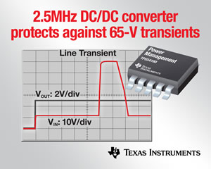
The TPS54160 non-synchronous buck's 3.5-V to 65-V input voltage range provides designers flexibility in applications with input transients. By leveraging TI's innovative Eco-mode™ light-load switching technique, the converter is able to achieve a low 116-uA operating current and 1.3-uA shutdown current, resulting in longer system run-times and a more efficient power system design.
In addition, the converter's high switching frequency range of 300 kHz to 2.5 MHz reduces the size of the output inductors to save board space. The TPS54160's frequency fold-back and thermal shutdown features allow the converter to protect itself during an overload condition.
The TPS54160 also has an integrated track pin that simplifies various sequencing schemes and a clock pin that reduces noise by synchronizing its switching frequency to an external clock.
TI's SWIFT DC/DC converters serve a broad range of applications, such as telecom, computing, industrial and consumer point of load applications with input voltage ranges as wide as 65-V and output currents as high as 14 A.
Pricing and availability
The TPS54160 is available today from TI and its authorized distributors in 10-pin MSOP PowerPAD™ packaging. Suggested resale pricing in 1,000-unit quantities is $2.40. Reference designs, evaluation modules and the SwitcherPro™ software tool for the TPS54160 are also available online at www.ti.com/tps54160evm.
From: http://ti.com
Freescale MEMS sensors enhance motion sensitivity in handheld devices
15:54Freescale Semiconductor has introduced two advanced 3-axis digital accelerometers to help mobile device developers meet the demand for sleeker, more sophisticated portable electronics products. Based on Freescale’s proven micro-electromechanical system (MEMS) technology, the MMA7455L and MMA7456L accelerometers enable low power consumption and motion sensing within a small form factor, making them ideal for cell phones and portable media players. The MEMS devices also can be used as drop-in replacements for customer designs already in production.
The MMA745xL 3-axis accelerometers provide digital output, a key capability that eliminates the need for an extra analog-to-digital (A/D) converter and enables flexible board layout options. The accelerometers also can be integrated directly to system processors for communication simplicity and flexibility. In addition, the sensors offer motion signature detection and pulse detection controlling device inputs and responses that are highly sensitive to natural human movement.
The MMA745xL accelerometers enable a variety of motion-sensing functions, such as tilt scrolling in all directions, gaming control, gesture recognition and tap to mute. The MMA745xL accelerometers also support functions such as theft protection, freefall detection and back-up GPS, as well as myriad other motion-based applications.
“As developers continue to add more sophisticated motion-based user interfaces to cell phones, cameras, MP3 players and other handheld devices, the demand for cost-effective MEMS-based accelerometers such as MMA745xL sensors is expected to grow,” said Demetre Kondylis, vice president and general manager of Freescale’s Sensor & Actuator Solutions Division. “Portable electronics developers also are looking for platform solutions to help them accelerate the design process and speed their products to market. Freescale’s latest ZSTAR3 demonstration board makes it fast and easy for developers to incorporate MEMS sensors and wireless technology into their next-generation designs.”
The MMA745xL accelerometers offer a broad range of sensitivity that covers 2g, 4g, and 8g, enabling greater design flexibility. The sensors are housed in an industry-leading ultra-thin 3 x 5 x 1.0 mm LGA package, which is ideal for space-constrained mobile applications.
Enabling quick design
To help wireless device manufacturers streamline the development process, Freescale has introduced the third edition of its popular wireless sensing triple-axis reference (ZSTAR) demonstration board. The ZSTAR3 kit accommodates multiple digital and analog accelerometer boards, connected through an RF ZigBee® 2.4 GHz communication interface to a single USB node connected to a PC. The accelerometer boards measure acceleration in three axes using a pin-compatible digital or, optionally, an analog sensor.
For high-performance mobile devices, Freescale offers an i.MX31 product development kit (PDK) that supports Microsoft’s Windows® CE 5.0, Windows Embedded 6.0 and Linux® operating systems. The i.MX31 PDK incorporates the 3-axis MMA7455L digital accelerometer that communicates directly to the i.MX31 system processor easing design integration.
For more information about Freescale’s accelerometer products and tools, visit www.freescale.com/files/pr/xyz.html.Development support, price and availability
The MMA7455L and MMA7456L sensors are available now. The suggested resale pricing in 10,000-piece quantities starts at $2.60 (USD) for MMA7455L and $2.70 (USD) for the MMA7456L.
The KIT3468MMA7455L and KIT3468MMA7456L development kits are available at a suggested resale price of $35 (USD) each.
ZSTAR3 reference platforms are available now. The platforms are available at a suggested resale price of $99 (USD) each.
The i.MX31 PDK is available now at a suggested resale price of $2,499 (USD).
From: http://freescale.com
Freescale strengthens radio frequency power transistor portfolio for commercial aerospac
15:53Freescale Semiconductor has reinforced its commitment to the commercial aerospace market with the introduction of a high-performance laterally diffused metal oxide semiconductor (LDMOS) RF power transistor. The latest addition to Freescale’s RF aerospace portfolio, the MRF6V4300N device is optimized for HF to UHF communications.
The MRF6V4300N power transistor is ideal for a wide range of applications, including radar and air traffic management systems. It is designed to deliver the highest gain and efficiency in its class. The device delivers RF output power of 300W CW from 10 MHz to 600 MHz. At 450 MHz, it has a gain of 22 dB and 60 percent efficiency.
“Freescale’s LDMOS RF devices have been proven in wireless and other applications around the world, and now we’re bringing their capabilities to the aerospace market where they are superior in performance to previous-generation devices currently in use,” said Gavin Woods, vice president of Freescale’s Radio Frequency Division. “In radar systems, bipolar junction transistors and vertical MOSFETs have been the device of choice for decades. However, their performance has not increased significantly over the years. In contrast, Freescale plans to continue enhancing the output power, frequency range, gain efficiency and ruggedness of its LDMOS technology for many years to come.”
Housed in Freescale’s RoHS compliant, cost-effective over molded plastic package, the MRF6V4300N device has exceptionally tight mechanical tolerances and an extremely low thermal resistance of 0.24 degrees Celsius per watt (C/W), which enhances the management of heat dissipation and helps reduce the heat sink size.
Freescale’s RF portfolio for aerospace
Earlier this year, Freescale introduced its first LDMOS RF devices for the commercial aerospace market for use in L-band radar applications. The MRF6V14300H 50V LDMOS field-effect transistor (FET) is designed to deliver up to 330W of pulsed output power from 1.2 to 1.4 GHz with 18 dB of gain and up to 60.5 percent drain efficiency, which is significantly better than the performance of bipolar junction transistors (BJTs) available for this frequency range.
The MRF6V14300H is accompanied by the MRF6V10010N, a driver amplifier that produces up to 10W of RF output power from 960 MHz to 1.4 GHz. When complemented by Freescale’s cost-effective MMG3014N pre-driver in a three-stage lineup, the trio of devices can deliver up to 330W of peak RF output power at 1.4 GHz (300 microsecond pulse, 12 percent duty cycle), with 62 dB of total gain, and an overall efficiency up to 59.5 percent including associated combining losses.
In addition, the MRF6VP41KH, introduced in 2007, is one of Freescale’s first LDMOS FETs to deliver 1 kW of RF power (100 microsecond pulse, 20 percent duty cycle). It has efficiency of up to 64 percent, 20 dB power gain at 450 MHz and can produce RF output power up to 1 kW at 1 dB compression.
These RF devices, along with the new MRF6V4300N, form a comprehensive portfolio with frequency coverage from HF through L-band. Freescale intends to continue to expand its RF portfolio in frequency and power with additional devices planned for announcement next year.
Freescale‘s aerospace RF devices incorporate electrostatic discharge (ESD) protection, which is engineered to provide exceptional resistance to damage caused by stray energy encountered on assembly lines. This capability also enables a broad gate voltage swing of -6 to +10V to help improve performance when the devices are operated in higher-efficiency modes such as Class C. The rugged devices are designed to handle high impedance mismatches ranging up to 10:1 VSWR at their rated RF output power when operated from 50V DC supplies.
Pricing and availability
The MRF6V4300N, MRF6V14300H, MRF6V10010N and MRF6VP11KH are in full production and supported by test fixtures. For more information about the MRF6V4300N device, visit www.freescale.com/files/pr/rf.html.
From: http://freescale.com
Agilent Technologies Introduces Industry's First Device Analyzer with Curve Tracer Functionality for Power-Device Evaluation
15:42Agilent Technologies Inc. today introduced the industry's first power device analyzer/curve tracer able to characterize semiconductor devices at up to 3,000 volts and 20 amps in a single box solution.
Power devices, including power management ICs (PMIC) and power MOSFETs and motor control ICs used in cars, are a growing device category that requires both high-power and high-accuracy test. In order to meet emerging standards for low-carbon emissions and improved energy efficiencies, power devices must function more efficiently even as they continue to become more complex, smaller and faster. New devices using wide band gap materials such as silicon carbide (SiC) or gallium nitride (GaN) have been widely studied in order to achieve high efficiency. To enable the careful and precise testing to meet performance and safety requirements, these studies require high-voltage measurement capabilities greater than 1,000 volts. In addition, for those power-device developments, on-wafer testing becomes very important for reducing development turnaround times.
Featuring a curve tracer mode, the Agilent B1505A can replace curve tracers used in failure analysis, as well as in circuit design or power module development of electronic equipment makers. It combines familiar curve tracer functionality with the convenience of a PC-based instrument, for improved ease-of-use and the ability to perform failure analysis of power device and power circuitry. The Windows(tm) PC-based B1505A allows users to export and store the measurement data easily, eliminating the measurement data handling and reporting limitations of traditional curve tracers.
"Accurate testing of high-power devices is a growing requirement for semiconductor manufacturers, and existing solutions do not offer the necessary voltage and current output," said Minoru Ebihara, vice president and general manager of Agilent Hachioji Semiconductor Test Division. "The B1505A is an integrated solution that provides researchers and device/process development engineers of power devices with high-voltage and high-current source and measurement capabilities, and its curve tracer mode makes it easy for users to take advantage of its PC-based EasyEXPERT software."
Key Features of the Agilent B1505A Power Device Analyzer/Curve Tracer
- Accurate measurement of breakdown voltage and leakage currents at high voltage.
- Evaluation of the low on-resistance of power devices at high current.
- Quick troubleshooting and analysis for failure analysis of these devices and power electronic circuitry.
- Device characterization at 3,000 volts and 20 amps in a single instrument
- Sub picoamp level measurement capability at high voltage.
- 50 microsecond current pulse width at high current, shortest current pulse width in the industry.
- Capacitance-Voltage (CV) measurement with up to 3,000 V bias.
- Quick device-check enabled by curve tracer mode.
- Easy operation and data management functions with PC-based EasyEXPERT software.
- On-wafer testing and prober control.
- Standard fixture with interlock creates safe measurement environment.
Modular Hardware and Accessories for Flexibility and Ease of Use
The B1505A has a 10-slot modular configuration that allows for customization and future expandability. It also supports two new modules: the B1512A high-current SMU (HCSMU) and the B1513A high-voltage SMU (HVSMU). The B1512A HCSMU can source and measure high-current, with support for up to 20 amps/20 volt pulse measurements. The B1513A HVSMU can source and measure high-voltage, with support for 3,000 volts (at 4 mA) and 1,500 volts (at 8 mA). In addition, the B1505A will support the B1510A high-power SMU (HPSMU) and B1520A multifrequency capacitance measurement unit (MFCMU) modules, which are currently available for the B1500A. A variety of external test fixtures and switching modules are supported to permit the safe testing of power devices and to allow switching between the B1505A's modules without having to change the cabling.
New EasyEXPERT 4.0
Agilent EasyEXPERT is the Windows PC-based software installed with the B1505A that enables easy operation through an intuitive GUI. EasyEXPERT 4.0, the newest version of Agilent's popular parametric test software, will be co-released with the B1505A. In addition to other enhancements, EasyEXPERT 4.0, which runs on both the B1500A and B1505A, can be controlled with a curve tracer-like rotary knob on the instrument. The EasyEXPERT 4.0 PC-based software will also be available in a Desktop version that can be run on an external PC in either online or offline modes, providing a unified parametric measurement environment for the B1500A, B1505A, 4155B/C and 4156B/C.
U.S. Pricing and Availability
The Agilent B1505A will be available for order beginning March 1, 2009. Pricing for Agilent B1505A will start at $45,000. An option will also be available to allow current B1500A users to convert their existing B1500A to a B1505A.
From: http://www.agilent.com
Agilent Technologies Introduces World's First Standalone High-Resolution LXI Digitizers
15:41Agilent Technologies Inc. today introduced the world's first standalone high-resolution digitizers with LXI connectivity for R&D and manufacturing engineers. These LXI digitizers are the choice of instruments when digital multimeters cannot sample fast enough, or oscilloscopes cannot provide high enough resolution for the waveform analysis requirements.
The Agilent L4532A 2-channel and L4534A 4-channel digitizers are new high-performance, stand-alone LXI digitizers that offer simultaneous sampling at up to 20 MS/s, and with 16-bit resolution. These products represent a new category of digitizers with their robust input channel and high performance analog-to-digital (A/D) design, and on-board measurements. The isolated input channels can measure up to 250V and are designed to handle demanding applications requiring electromechanical device control for product test or characterization.
"Engineers deal with test challenges every day, like reading low voltages within high-voltage signals," said Gary Whitman, vice president and general manager of Agilent's System Products Division. "This requires them to develop signal conditioning prior to using instruments and question the accuracy and stability of the test instruments they are using. The new L4532A and L4534A digitizers address these needs by providing high performance, isolated input channels with voltage inputs up to 250V. The digitizers also provide the long-term accuracy and stability that customers expect from Agilent products."
The new Agilent high-resolution LXI digitizers were designed with input from engineers on waveform analysis in automotive, aerospace/defense, communications and medical applications. As a result of this input, the high-performance design, with a choice of noise filters, has reduced the need to add expensive signal conditioning prior to digitizing waveforms. The digitizers include on-board "scope-like" measurements such as Vmin/Vmax, Vp-p, frequency and rise/fall time that can be applied to a selected portion or the overall waveform. The on-board measurements save post-processing time and minimize the need to transfer and store large amounts of data.
The Agilent L4532A and L4534A are fully compliant with the LXI class C specification. They include USB 2.0, and Gigabit Ethernet (LAN) interfaces as standard features, enabling quick and simple connectivity to a PC or a network. In addition, they can be remotely operated from any browser by simply connecting to the built-in Web page.
U.S. Pricing and Availability
The Agilent L4532A 2 channel 20MS/s digitizer is priced at $6,500, and the L4534A 4 channel 20MS/s digitizer is $8,500. Extended memory is an additional $1,500. The digitizers are available for order now and will be shipped in December 2008.
From: http://www.agilent.com
National Instruments Announces Plans to Expand Global Presence With New R&D and Operations Facility in Malaysia
15:39National Instruments today announced plans to open a new R&D and operations facility in Malaysia in 2010. An $80 million capital investment, the new facility will occupy 17 acres on the island of Penang and eventually employ 1,500 people in manufacturing, product development, R&D, shared services, IT and finance positions. National Instruments is developing the facility as part of the company’s ongoing plan to expand global operations to support the company’s growth.
“Hundreds of thousands of engineers and scientists around the world have adopted National Instruments software and hardware to develop innovative applications, resulting in strong, long-term growth for our company,” said Dr. James Truchard, president, CEO and cofounder of National Instruments. “The new facility will help us better serve our customers and support the continued growth of our business while giving us access to the great talent that Malaysia and Penang have to offer.”
Founded in 1976, National Instruments develops and manufactures software and hardware products that engineers and scientists use for test, control and embedded design applications. The company’s graphical system design tools, which combine the open NI LabVIEW software with commercial off-the-shelf programmable hardware such as NI CompactRIO and PXI, give engineers and scientists a complete development platform for designing, prototyping and deploying systems more rapidly than traditional methodologies.
“We are excited to welcome National Instruments to Malaysia and honored the company has chosen to invest in our country,” said Tan Sri Muhyiddin Yassin, minister of international trade and industry in Malaysia. “Malaysia offers a talent-rich, competitive environment that is ideal for higher value-add companies, and we look forward to a successful collaboration with National Instruments.”
Malaysia’s strong university system, skilled engineers and IT professionals, regional infrastructure, favorable business climate and proven success of supporting global high-tech companies attracted National Instruments to the country. The close proximity of the new facility to Asian markets also makes it possible for the company to respond more quickly to customer demand in the region and provide better access to software and hardware services such as product calibration.
“After an extensive, multi-year search, National Instruments selected Malaysia as the site of our new R&D and operations facility because of its skilled workforce, cost-competitive environment and quality support from national and local officials,” said Rob Porterfield, vice president of manufacturing at National Instruments. “We want to thank the Malaysian Industrial Development Authority and Invest Penang for their professional assistance in helping us realize our plans for the facility.”
National Instruments has a very strong financial track record, with more than $276 million in cash and short-term investments, and has been consistently profitable since 1990. With record revenue of $740 million in 2007, the company has delivered revenue growth for 30 of its 31 years. A key driver of the company’s growth has been its long-term commitment to R&D, which has consistently provided disruptive innovations in the test and measurement and industrial and embedded target markets. National Instruments employs more than 5,000 people worldwide including more than 1,400 in R&D.
“As a global leader in technology, National Instruments is a welcome addition to Penang and will bring high-value jobs to our state,” said Lim Guan Eng, chief minister of Penang. “Penang has a proven history of successful business development, and we are confident that the people and resources of Penang will offer tremendous value to National Instruments.
New Tektronix MPEG Test Analyzers Foster DTV and IP Video Transition
15:23Tektronix, Inc., a leading, worldwide provider of test, measurement and monitoring instrumentation, announced two new models in the MTS400 MPEG Analyzer Series. The midrange MTS415 and the portable, entry-level MTS400P models provide first line diagnostics with integrated cross layer fault analysis and error logging. Additionally, the company announced an enhancement to the MTS430 and new Tclips test streams. The analyzers add to the industry-leading portfolio of video test equipment and solutions from Tektronix with a wide range of supported DTV and IP Video related standards including MPEG, DVB, ATSC, ISDB-T, ISDB-TB, IPv4 and IPv6. The new additions advance the development and deployment of next generation DTV and IP Video networks and services.
Engineers developing, testing, debugging and evaluating next generation compressed video technology, products and services that are distributed and delivered over RF and/or IP networks must comprehensively and quickly test, characterize, and validate video services within their systems. Broadcasters, Network Operators and Cable MSOs need to ensure high availability network performance and improve their time to insight when problems arise. Tektronix provides a complementary suite of MPEG analyzers, generators and monitors with a common analysis engine for monitoring and analysis activities to meet these diverse and demanding needs.
“The first step for an engineer troubleshooting a problem in a digital broadcast system is always to narrow a fault down to the source,” said Paul Robinson, senior manager MPEG test segment, Video Product Line, Tektronix. “Detailed analysis at the appropriate layer can only be performed once the source of the problem is identified. The new portable MTS400P and mid-range MTS415 video analyzers extend the industry-leading Tektronix portfolio of complementary MPEG analyzers, generators and monitors.”
The portable MTS400P real-time analyzer provides an entry-level MPEG analyzer from the leading video test vendor. In addition to standard features, the IP Video Option for the MTS400P offers a choice of 10, 100 and 1000base-T or optical Line Rate connections. This option supports IPv4 and IPv6 networks and includes Time-stamped Transport Stream (TTS) analysis. The MTS400P enables customers to analyze both constant and variable bit rate streams, single or multi-program transport streams plus IP and TS Key Performance Indicator analysis of up to 500 simultaneous sessions in IPv4 and IPv6 based networks. Other options include an MPEG Player, Deferred Time Multiplexer, Deferred Time Transport Stream Compliance Analyzer, PES Analyzer, Buffer Analyzer and a Carousel Analyzer and Generator.
The new MTS415 offers premium analysis and the key measurements that broadcasters and operators require. Standard features include an MPEG Player / Recorder, Transport Stream Compliance Analyzer for either deferred time or real time analysis, PES and Buffer Analyzers. Also included is MTS4CC, a cost effective solution for CODEC comparisons and diagnosing interoperability problems. Like the MTS400P, an IP Video option is available for the MTS415 that includes support for IPv6 and Time-stamped Transport Stream Analysis.
The MTS415 provides first line diagnostics with integrated cross layer fault analysis and error logging. Time to problem insight is reduced by informing the user whether root cause of video problems is at the Transmission, Transport Stream or Elementary Stream layer. With its new measurement interfaces and analysis capabilities, the MTS415 Series is ideal for equipment developers working to improve product quality and reduce time to market and assists engineers and technicians within broadcasters and network operators looking to ensure quality of service in next generation video networks.
The MTS430 provides a fast analysis engine, enabling reduced time to insight, rapid development, evaluation, deployment and diagnostics of next generation DTV and IPTV systems and services. New MTS430 models now include a second software license that allows either the TS or ES analysis tools to be used on another PC.
Updated MTS400 Series analysis software includes a number of new advanced capabilities including PCR-PTS cross layer timing analysis to identify encoder access unit timing errors as well as Boolean packet searching which simplifies tracking down complex issues such as incorrect conditional access signaling.
Tclips are a broad range of MPEG-2 Transport Streams designed to test receivers across a broad range of video and audio formats. Tclips test streams are designed to test the receivers to the limits of their abilities and will be included as standard with all new MTS415 and MTS430 analyzers. When used in combination with the Tektronix Software Multiplexer, the test streams can be adapted to the specific needs of the user.
Availability
The MTS400P, MTS415, Tclips and enhanced MTS430 will be available for order in December 2008 with shipments in early 2009. Entry-level pricing for the MTS400P begins at $14,000, U.S. MSRP. Tclips will also be available as a separate standalone product to complement the current MTS4SA and MTS400 units. Additional information about the MTS400 Series can be found at: www.tektronix.com.
From: http://www.tektronix.com
Tektronix MPEG Video Monitor Provides Enhanced IP Video and DTV Quality of Service Capabilities
15:21Tektronix, Inc., a leading, worldwide provider of test, measurement and monitoring instrumentation, announced additional features for the MTM400A MPEG Transport Stream Monitor. Key amongst these are support for Variable Bit Rate (VBR) corrected measurements, a “monitoring by exception” Learning Mode and Video and Audio Backhaul. Part of the extensive Tektronix video test equipment platform, the MTM400A enables broadcasters and network operators to better detect signal degradation caused during transmission and distribution to find and diagnose errors more quickly to prevent viewers from experiencing loss of signal.
The worldwide DTV market continues to evolve and a second wave of DTV services are now actively being rolled out leveraging IP technology as the delivery mechanism for video distribution, contribution and broadcast services. Shifting consumer viewing behavior combined with increasing competitive pressure is driving an explosion in broadcast channel count and overall capex investment. A key operational challenge for traditional broadcasters and Multi-Service Operators (MSO) is how to efficiently deliver superior Quality of Service (QoS) levels to maintain differentiation in this competitive market. The MTM400A supports this by providing an intuitive and simplified presentation of video quality and diagnostic information, to enable delivery of superior QoS levels in an increasingly complex broadcast environment.
Measurements defined in TR 101 290 are intended to be applied to Constant Bit Rate (CBR) transport streams and support in-depth analysis of Transport Stream, syntax, timing and content to support root cause analysis of system errors. Simply applying these measurements to a VBR stream places measurement results in doubt. The MTM400A converts VBR streams to CBR streams before applying TR 101 290 measurements, ensuring highly reliable results.
The Learning Mode on the MTM400A provides an unattended methodology to “teach” the monitoring system about the steady state conditions of the operating environment. The MTM400A learns to alarm on unacceptable changes in these steady state conditions and monitor by exception instead of simply responding to out of specification parameters that don’t directly impact QoS.
A critical aspect of ensuring QoS is the ability to see and hear what is actually being transmitted. The MTM400A is now supports video and audio backhaul, with the user being able to select either the entire program or just the audio for decode on the controlling PC. Alternatively, the backhauled content can be directed to a set top box for hardware decode, a capability that is particularly useful with encrypted content.
In addition to VBR Corrected Measurements, Learning Mode and Video/Audio Backhaul, the line rate IP interface of the MTM400A now supports IPv6 -- the latest generation of Internet Protocol (IP) -- and provides enhanced capabilities for IGMP, the protocol used by IPv4 systems to report IP multicast group memberships to neighboring multicast routers. Also, the multi-session IP Video KPIs of the MTM400A have been extended to include max/min session bit rate alarms as well as enhanced support for Media Delivery Index (MDI). MDI is important for monitoring CBR MPEG Transport Streams distributed over IP networks in conjunction with reliable TR 101 290 and other TS measurements. These measurements have been extended to include PCR-PTS cross layer timing analysis, intended to identify encoder timing issues in real time.
The MTM400A with the powerful FlexVuPlusTM user interface leverages the deep measurement capabilities of the MTM platform to deliver greatly simplified DTV monitoring and diagnostics. The MTM400A with FlexVuPlus provides a configurable common user interface for both confidence and diagnostic monitoring that improves communication handover between operator and engineer.
“Video Service Providers need measurement and monitoring solutions that provide greater capabilities and more intuitive operation,” said Paul Robinson, senior manager MPEG test segment, Video Product Line, Tektronix. The MTM400A is a real time, high availability monitoring probe that provides capability for broad and shallow KPI-based confidence monitoring as well as narrow and deep diagnostic measurement capability to facilitate reduced times to insight and fast error correction. The additional features now available in the MTM400A such as VBR corrected measurements and exception monitoring help our customers achieve a faster understanding of initial fault reporting, accelerating time to overall problem resolution.”
Availability
The MTM400A is available for order and delivery of the new features will begin in early 2009. Upgraded software will also be available as a free of charge upgrade for existing MTM400A owners.Fujitsu Laboratories Develops C- to X- Ultra-Wideband Gallium-Nitride HEMT Power Amplifier Featuring High Output and Efficiency
14:31Fujitsu Laboratories Ltd. announced today the development of a high-performance power amplifier based on gallium nitride (GaN) high electron mobility transistors (HEMT), which as a hybrid amplifier - an amplifier in which the transistor and capacitor are each mounted on separate semiconductor package substrates - features the world's highest output performance in terms of power and efficiency in the C-band to X-band radio frequency bandwidths above 5GHz. This technology opens the potential for higher performance and functionality in broadband and radar communication systems, in particular for airplane radar systems and other instruments that use multiple frequencies, which could be accommodated by a single amplifier. Furthermore, in comparison with conventional power amplifiers that use gallium-arsenide (GaAs), the new ultra-wideband (UWB) GaN-HEMT-based amplifier features higher efficiency, thus enabling a reduction in the size of cooling equipment, which is anticipated to result in power amplifiers that are smaller and lighter.
Details of this new technology were presented at the 2008 IEEE Compound Semiconductor IC Symposium (CSICS), held in Monterey, California from October 12-15.
Background
In order to expand radar detection ranges and the distance that radio waves in wireless communications can travel, it is necessary to increase the output power of transmitters. In addition, in order increase transmission capacities and heighten the detection performance of radar that detects multiple targets, it is necessary to expand the bandwidth of transmitters and enable them to handle multiple channels. Airplane radar systems need to use two different types of transmitters so they can switch back and forth between the C-band, which is relatively impervious to the effect of atmospheric precipitation, and the X-band, which enables high-resolution measurement. If a transmitter could handle ultra-wideband frequencies spanning from the C-band to the X-band, then just one transmitter would suffice, which would enable systems that are more compact.
Conventionally, GaAs transistors have been used in wideband high-output amplifiers; however the output of many GaAs transistors needs to be combined in order to generate sufficient transmission output, leading to a reduction in efficiency as a result of losses in the matching circuit. Therefore, instead of GaAs, in recent years there has been a surge in efforts to develop GaN-based HEMT amplifiers which have a larger dielectric breakdown field and the potential to generate higher output levels.
Technological Challenges
It is widely known that monolithic microwave integrated circuits (MMICs) - which include a transistor, capacitor, resistor, and circuit interconnects all mounted on the same semiconductor substrate - enable wideband characteristics at high frequencies such as the C- and X-band range. However, due to the aforementioned problems faced when using GaAs transistors, MMICs using GaAs have been unable to deliver sufficient levels of output and efficiency.
On the other hand, in trying to apply MMIC technology to GaN HEMTs which feature high operation voltages, the breakdown voltage of the chip capacitor has been insufficient. By using a hybrid integrated circuit instead, in which the transistor and capacitor are mounted separately, the impedance problem is eliminated because a high-breakdown voltage-capacitor can be used. However, as wires used in the signal line connections or ground connections reduce the amplification factor of high-frequency signals, thereby increasing frequency variance, it has been thus far difficult to generate high efficiency in a wide bandwidth.
Newly-Developed Technology
Fujitsu Laboratories developed a C- to X-band hybrid GaN HEMT power amplifier that resolves the aforementioned issues. Key features of the technology include the following:
- Although wires used in ground connections reduce the amplification factor of high-frequency signals used in the C- to X-band range, in the newly-developed hybrid circuit a transistor with via holes that connect the GaN HEMT chip's surface electrode with the bottom electrode (Figure 1) is used, thus eliminating the need for ground connection wires and thereby suppressing reduction of the amplification factor of high-frequency signals.
- In order to suppress the frequency variance caused by wires used in the signal line connection, a UWB matching circuit was developed. Furthermore, by employing a high-breakdown-voltage capacitor in the matching circuit, high output power was achieved at high operating voltages.
These technologies enabled the generation of both high output power and high efficiency at high frequencies across wide bandwidth. In addition, although it is a hybrid power amplifier, the new amplifier is compact, measuring just 6.0mm x 6.6mm (Figure 2).
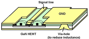
Figure 1: Diagram of a GaN HEMT chip with via-holes
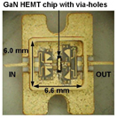
Figure 2: Newly developed C- to X-band power amplifier

Figure 3: Efficiency comparison of UWB GaN-hybrid C- to X-band power amplifiers
Results
The newly-developed UWB hybrid C- to X-band power amplifier achieved output of 6.5W and efficiency of 40% at a lower-range frequency of 7 GHz, and achieved output of 4.1W and efficiency of 26% at the higher-range frequency of 12 GHz. These results significantly exceed previously-reported performance levels for UWB GaN-based high-output hybrid amplifiers resulting in the world's highest level of performance (Figure 3).
This technology enables transmitters to handle multiple channels and enables the use of multiple frequencies with differing characteristics, opening the horizon to communication systems that can offer higher performance and functionality, such as broadband communications and radar systems that can use multiple frequencies. The technology can also be used in measuring instruments, for which output at high frequencies had been insufficient, in order to measure the performance of amplifiers used in broadband communications and radar systems. Moreover, because the new GaN-HEMT-based amplifiers are more efficient than conventional amplifiers using GaAs, it is expected that reductions in size and weight of the equipment box, which houses the amplifier and cooling system, can be made possible.
Future Developments
Fujitsu plans to widely use this technology in areas that require high-output broadband performance, such as wireless communications equipment and radar systems.
From: http://www.fujitsu.com
Fujitsu MHZ2 CJ Series of 2.5” HDDs Earns JIS Security Accreditation
14:29Fujitsu Limited and Fujitsu Laboratories Ltd. today announced that the MHZ2 CJ Series of 2.5” hard disk drives (HDDs) with automatic hardware-based encryption, introduced by Fujitsu in April 2008, has become the first HDD line to obtain JIS X 19790 Security Accreditation. The accreditation means that these products have met one of the major standards for data security required for the procurement of IT products by government agencies in Japan and signifies that the MHZ2 CJ Series provides the level of data security required by all public agencies in Japan.
In April 2008, Fujitsu announced the MHZ2 CJ Series of 2.5” HDDs. This new series, complying with the 256-bit Advanced Encryption Standard (AES), aims to prevent information leakage from lost or stolen notebook computers and external HDDs.
The MHZ2 CJ Series has now become the first series of HDDs to obtain accreditation under the JIS X 19790 accreditation program - the Japan Cryptographic Module Validation Program (JCMVP).
JCMVP accreditation is granted to products equipped with the appropriate cryptographic algorithms and acting as cryptographic modules to ensure the security of important information such as the encryption key.
In February 2008, the National Information Security Center issued the "Standards for Information Security Measures for the Central Government Computer Systems (Third Edition)."According to the section on "Introducing the Functions for Encryption and Performing Electronic Signatures," selecting products with JCMVP accreditation is an enhanced requirement. With JCMVP accreditation, the MHZ2 CJ Series will contribute to enhancing the security of IT products and system deployments for our customers in both private and public sectors.
Fujitsu is a leader in the design and development of HDDs with next-generation security features. In June 2008, the company was elevated to the status of Promoter Member of the Trusted Computing Group (TCG), which works to develop and disseminate industry standards for security-related technologies. Leveraging its accumulated technology and know-how, Fujitsu will continue offering products that meet its customers’ needs for information security.
From: http://www.fujitsu.com