
Archive : 12 November 2008 year
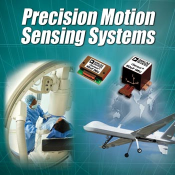
ANALOG DEVICES’ INERTIAL SENSORS DELIVER COST-EFFECTIVE, EASY-TO-IMPLEMENT MOTION SENSING FOR INDUSTRIAL AND MEDICAL INSTRUMENTATION
21:00Analog Devices, Inc. a global leader in high-performance semiconductors for signal processing applications, is expanding its award-winning iSensor™ intelligent sensor product family with two new inertial sensors that make it simple and affordable to implement sophisticated motion and navigation control in a broader range of applications, including medical instrumentation. The ADIS16405 six-degrees-of-freedom (6DoF) inertial measurement unit (IMU) combines high-performance, simplicity, and a tri-axis magnetometer sensor for improved heading accuracy. The ADIS16300 four-degrees-of-freedom (4DoF) IMU is offered at an industry breakthrough price that is up to 10 times less than other products in its class.
“Analog Devices’ iSensor intelligent sensor IMU portfolio has opened new markets and applications for advanced motion sensors,” said Bob Scannell, business development manager, iSensor intelligent sensor products, Analog Devices. “The ADIS16405, which offers pre-calibrated and pre-aligned inertial and magnetic sensors, greatly simplifies the process of implementing full IMU sensor functionality. The industry’s lowest cost, precision multi-axis inertial sensor, the ADIS16300, enables a broad array of new applications, including medical imaging equipment, prosthetics, surgical instrumentation, and industrial vehicle navigation. These products, along with other offerings available in ADI’s IMU portfolio, provide customers with pin-compatible options that give them complete choice and flexibility in meeting multiple cost/performance needs.”
About the ADIS16405 iSensor Intelligent Sensor
Designed using Analog Devices’ world-class iMEMS® Motion Signal Processing Technology™, the ADIS16405 complete inertial sensing system integrates a three-axis gyroscope, magnetometer, and accelerometer. The embedded magnetometer provides accurate heading to complement the product’s superior response and short-term stability.
Unlike many IMUs, which offer a lower level of integration and require a high degree of user calibration, all necessary motion testing and calibration for the ADIS16405 is performed at the factory. This means that system integration time is greatly reduced and customer implementation is as simple as supplying power and connecting an SPI (serial peripheral interface) port. This enables systems designers to reduce their system development time by up to a year while saving hundreds of thousands of dollars in test equipment capital costs.
The ADIS16405 features 0.05 degree rate-sensor orthogonal-alignment-accuracy, which improves overall system accuracy and simplifies end-system design. The magnetometer sensors are calibrated and aligned to the inertial sensor axis. The extensive calibration and dynamic compensation results in an angular random walk of below 2.0 degrees/√hr and temperature stability of 40 ppm/°C. All sensors are accessible over a standard SPI interface, which also allows control of internal digital filtering.
About the ADIS16300 iSensor Intelligent Sensor
Offered at a fraction of the cost of competing devices, the ADIS16300 complete inertial sensing system integrates a single-axis gyroscope and a three-axis accelerometer. Each sensor in the ADIS16300 combines ADI’s iMEMS technology with signal conditioning that optimizes dynamic performance. The factory calibration characterizes each sensor for sensitivity, bias, alignment, and linear acceleration. As a result, each sensor has its own dynamic compensation which results in accurate sensor measurements over the specified power supply range of 4.75 V to 5.25 V. As with the ADIS16405, factory calibration of the ADIS16300 greatly reduces system integration time and test equipment costs. Similar to the ADIS16405, the ADIS16300 features an improved SPI interface to provide faster data collection and configuration control.
Angular rate sensing can be selected for ±75, ±150, and ±300 deg/sec dynamic range, with ±3 g tri-axis acceleration dynamic range. The device offers a 350-Hz bandwidth, and up to 1,200-SPS sample rates, with further digital filtering embedded and programmable. The ADIS16300’s flexible mounting approach also makes it easier to implement roll and pitch axis rate sensing.
The ADIS16300 and ADIS16405 are compatible with other iSensor multi-axis inertial sensors which include the ADIS16365, ADIS16364, ADIS16355, ADIS16354, and ADIS16350.
Availability and Pricing
1,000-Unit Quantities |
|||
| ADIS16405 | |||
| ADIS16300 |
For more information, visit http://www.analog.com/pr/ADIS16405 or http://www.analog.com/pr/ADIS16300.
Infineon Launches Intelligent Lamp Ballast Controller for Fluorescent Lamps
20:57Today at the electronica Trade Show, Infineon Technologies AG (FSE/NYSE: IFX) launched its next-generation lamp ballast controller that features intelligent digital/mixed signal power control. The new ICB2FL01G lamp ballast controller integrates Power Factor Correction (PFC), lamp controller and high-voltage half-bridge driver functions into a single, compact, surface-mounted package. Employing digital/mixed signal power control technologies, the product integrates all of the lamp start, run and protection features required by current and future fluorescent lamp ballasts. Reliable and robust high-voltage isolation is achieved using Infineon’s proprietary Coreless Transformer Technology (CLT). CLT is by nature an intrinsically robust high-voltage isolation media and offers excellent immunity from positive as well as negative transients.
Typical applications for the ICB2FL01G product are electronic ballasts for compact fluorescent lamps, linear fluorescent T5 and T8 lamps, dimmable fluorescent lamps and emergency lighting.
Digital / mixed signal power control enables stable, dependable ballast designs to be implemented with the minimum of external components and at minimum system cost. Depending on the application, more than 20 components, including capacitors, diodes and resistors can be saved. Furthermore, the use of this technology allows parameters to be set utilizing only resistors, which avoids the issues with trimming and aging associated with the use of capacitors in existing solutions. With few additional external components the ICB2FL01G supports multi-lamp designs controlling up to four lamps as well as multi-power ballast designs handling different power lamps. A key new feature of the second generation ballast controller is the provision of special built-in test modes that allow ballast manufacturers to dramatically shorten production test times, halving the time for key tests such as End-of-Life detection and preheat operation modes.
Further key features of Infineon’s ICB2FL01G lamp ballast controller include a wide programmable preheat time spanning from 0 ms to 2500 ms, which allows lamp ballast designers to support a wide range of lamps, as well as highly accurate timing and frequency control over a wide temperature range of -25 °C to +125 °C.
More and more emphasis is being placed not only on the efficient production of light, but also on its effective use. With this in mind, the ICB2FL01G has been designed to be highly compatible with dimmable lamp ballasts, offering outstanding efficiency (up to 90 percent) and THD (Total Harmonic Distortion) performance over a wide load range. Intelligent lamp fault detection and restart control enable compliance with Emergency Lighting requirements according to the European DIN VDE 0108 standard.
“Today, around one third of all energy consumption is electrical energy and around 15 percent of this is consumed by lighting, creating a growing demand for efficient lighting systems,” said Sandro Cerato, Vice President and General Manager, ASIC & Power IC at the Industrial & Multimarket division of Infineon Technologies. “Infineon plays a leading role in this area with a wide range of established products for fluorescent, high-intensity discharge (HID) and solid-state lighting applications, and this leading role is now further expanded with the launch of our ICB2FL01G next generation smart ballast controller that offers reliable and stable ballast designs at reduced system cost and with significantly reduced test times.”
Availability and pricing
The ICB2FL01G lamp ballast controller is sampling now. It comes in a standard lead-free DSO package with 19 pins. Volume production is scheduled for January 2009. A fully featured demo board is available and the product is supported by comprehensive application documentation.
National Instruments Adds Instrument-Class I/O to LabVIEW FPGA Hardware
20:52National Instruments today introduced a new family of open, FPGA-based hardware for the PXI platform. The NI FlexRIO product family is the industry’s first commercial off-the-shelf (COTS) solution to provide engineers with the flexibility of NI LabVIEW FPGA technology combined with high-speed, instrument-class I/O. With NI FlexRIO, engineers can add custom signal processing algorithms to their PXI-based field-programmable gate array (FPGA) hardware. Then, with interchangeable adapter modules, they can directly interface the FPGA to instrument-class I/O or create their own custom front-end hardware to meet their specific application requirements. With these capabilities, engineers can employ techniques such as in-line processing, hardware-in-the-loop (HIL) simulation and protocol-aware test required during the design and testing of many complex electronic devices.
“LabVIEW FPGA technology will continue to transform instrumentation and extend graphical system design by providing software programmability at the hardware level,” said Dr. James Truchard, president, CEO and cofounder of National Instruments. “NI FlexRIO gives engineers a way to solve applications that were previously impossible with COTS hardware.”
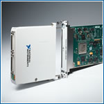
NI FlexRIO FPGA modules feature high-performance Xilinx Virtex-5 FPGAs that engineers can program using the LabVIEW FPGA Module. Previously, FPGA technology was limited to a subset of hardware engineers with extensive knowledge in digital design, but LabVIEW FPGA makes this technology available to all engineers through intuitive graphical programming. Using LabVIEW FPGA, engineers gain direct access to raw digital pins on the NI FlexRIO FPGA modules, with 66 differential lines at up to 1 Gb/s per pair or 132 single-ended lines at up to 400 Mb/s. In addition, NI FlexRIO FPGA modules offer deep onboard memory and the ability to use external clocks.
All NI FlexRIO implementations require two distinct hardware pieces – a PXI FPGA module and an adapter module, which defines the specific I/O capabilities of the system. The first NI FlexRIO adapter module is the NI 6581 high-speed digital I/O adapter, which is ideal for algorithmic pattern generation and protocol-aware tests. The NI 6581 delivers 100 MHz of digital I/O (200 Mb/s DDR) through 54 single-ended channels with selectable voltage levels including 1.8 V, 2.5 V and 3.3 V (5 V compatible). National Instruments also has worked with Averna to create a plug-and-play IEEE 1394b adapter module, and expects many additional modules to be available from third parties in the future.
Additionally, NI FlexRIO offers engineers the flexibility to design their own custom adapter modules with the exact converters, buffers, clocks and connectors to meet their application needs. To help engineers develop their own module configurations, the NI FlexRIO Adapter Module Development Kit (MDK) features full documentation on electrical and mechanical design details, including CAD files and PCB outlines as well as various adapter module metal enclosures.
For more information and a four-minute video about NI FlexRIO, readers may visit www.ni.com/flexrio.
Tektronix Video Test Solution Wins Outstanding Technology Award
20:50Tektronix, Inc., a leading worldwide provider of test, measurement and monitoring instrumentation, announced that its 3Gb/s Serial Digital Interface (SDI) Test Solution has received the prestigious Outstanding Technology Award at 2008 Beijing International Radio Film & Television Equipment Exhibition (BIRTV 2008). The award recognizes the technical breakthrough the company has achieved as the industry-first 3Gb/s SDI end-to-end test solution. Tektronix showcased this award winning solution along with a comprehensive portfolio of video test solutions for file-based video, MPEG, and HD technologies at Stand #3008 Hall 3 at BIRTV 2008, November 5 - 8 in the China International Exhibition Center, Beijing.
Supporting both A level and B level 1080p SMPTE formats, the Tektronix 3Gb/s SDI Test Solution is a combination of successful TG700 Series Generators and WFM7020/7120 Series Waveform Monitors with the 3Gb/s Single Link SDI support. The TG700 is a modular multi-format precision signal generation platform used by customers worldwide. It was recently used by NBC for the network’s coverage of the Beijing 2008 Olympic Games. With the new HD3G7 module for 3Gb/s SDI test signals, the TG700 supports 1080p formats to assist video equipment designers and manufacturers to get their products to market quickly and efficiently, and facilitates early roll out of 3Gbps services for broadcasters and post production operators. The new 3G (3Gb/s) and JIT (jitter for 3Gb/s) options for the WFM7120 monitor also provides an ideal test platform for fast verification of the 3Gb/s signal.
“Tektronix is well-recognized for its commitment to introducing innovative video test solutions and support for emerging technologies to meet the needs of new digital video applications,” said Zhang Hong, president of Cable TV Institute, Academy of Broadcasting Planning, SARFT. “We selected the Tektronix 3Gb/s SDI Test Solution for the BIRTV Outstanding Technology Award due to its unique capabilities and timeliness. The solution provides customers with great flexibility to quickly upgrade to 3Gb/s SDI standard compliant systems.”
"It is a great honor to receive the 2008 Outstanding Technology Award from BIRTV,” said James Alderton, marketing director, Tektronix Asia Pacific. “The video and TV broadcast industry is experiencing a revolutionary shift to digital and high definition technology. With the world's first 3Gb/s SDI end-to-end test solution, Tektronix is the preferred choice for technology companies who are developing products for high quality video distribution and broadcasting."
Other highlights on the Tektronix stand include:
- TG700 with GPS-based Synchronization and Timecode Generation supported by GPS7 module
- The latest Tektronix MPEG solution; the MTM400A MPEG Transport Stream Monitor. The MTM400A features the powerful FlexVuPlusTM user interface that leverages the deep measurement capabilities of the MTM platform to deliver greatly simplified DTV monitoring and diagnostics.
- Cerify®, the world’s first fully automated system capable of verifying the quality of file-based, compressed digital video and audio content prior to transmission or use.
- The award winning PQA500 that provides the most complete suite of measurement and diagnostic tools for picture quality analysis including full support of high definition (HD) formats.
- New IPTV Monitoring Solution
Medical imaging equipment OEMs can achieve faster, more accurate results with TI's portfolio of embedded processors and analog products
18:10Texas Instruments [NYSE: TXN] (TI) today announced a portfolio of more than 15 dedicated embedded processors which enable faster, more accurate results for doctors and clinicians while empowering imaging equipment manufacturers to develop new modalities or to make existing products smaller and more portable. These processors target several medical imaging applications including ultrasound, computed tomography (CT), positron emission tomography (PET), magnetic resonance imaging (MRI), digital x-ray, optical coherence tomography (OCT) and other newly developed modalities. The processors join with TI's full range of catalog and application-specific analog products to deliver a complete signal chain solution and help increase the speed and availability of care to millions of people around the world. For more information on the processors or TI's new family of ultrasound transmitters, go to www.ti.com/medicalimaging.
Faster, more accurate care
Embedded digital signal processors are flexible, programmable devices that can be field upgraded with the updated software and algorithms. Universities, programmers and R&D centers continually develop new algorithms to improve the clarity, depth and usefulness of diagnostic images. With TI's extensible processors, these new algorithms can be easily uploaded to field-deployed machines. For equipment manufacturers, these rapid updates lengthen the life of their installations, while improving machine functionality. For clinicians and patients, improved images equal better diagnoses and care response.
In addition to enabling improved images, TI's processors and high-performance analog products also positively impact the speed of care. Many of TI's integrated circuits for medical imaging offer exceptional performance at very low power and in ultra-small form factors, enabling equipment manufacturers to turn large, fixed machines into portable or handheld devices. Portable imaging machines can travel directly to the patient - whether in an ambulance, in remote locations or in trauma and triage settings - improving the overall speed and effectiveness of delivering treatment.
Embedded processors, as well as TI's DLP™ technology, also give manufacturers tools for new imaging modalities. New techniques such as tissue elasticity imaging, hyperspectral imaging, adaptive patient-specific imaging and 3D/4D imaging and vein viewing all leverage the numerous capabilities of high performance, low power devices from TI. For example, real-time, patient-specific tissue elasticity images can be achieved with new algorithms developed specifically for TI's processors, delivering optimal diagnostics. For 3D/4D imaging, which requires a tremendous amount of real-time processing, TI's processors improve the richness of 3D fetal modeling for clinical analysis and enable effective 4D cardiovascular applications. DLP technology eliminates "bad sticks" by allowing the patient's veins to be highlighted and easily viewed.
"Since the 1980s, TI has worked with medical customers and imaging pioneers such as the University of Washington to develop technologies that advance medical electronics to improve patient care," said Niels Anderskouv, Vice President, DSP Systems with TI. "With this portfolio of processors, we believe we are truly able to give our customers the tools they need to deliver faster, more accurate imaging results to patients and physicians."
Addressing many challenges facing imaging OEMs, TI begins with the signal chain - taking the analog signal captured by the machine, digitizing it for analysis and then converting it back to analog for viewing by the physician or clinician. Surrounding the signal chain, TI also provides power management, clocks, interface, amplifiers and data converters, resulting in the broadest semiconductor portfolio products available for all medical imaging modalities.
TI's embedded processors range from high-performance multicore devices to very low- power products that meet the imaging equipment manufacturers' needs. For example, TI's numerous multicore products offer significant computational performance required by OEMs for high-end imaging modalities. High-performance single-core processors such as the TMS320C6455 and TMS320C6452 are well-suited for imaging modalities requiring real-time operations such as ultrasound, digital x-ray, OCT, hyperspectral imaging and other emerging applications. Leveraging TI's industry-recognized imaging capabilities, the TMS320DM644x family improves backend processing for imaging applications. Portable and handheld applications benefit from TI's low power OMAP™ and TMS320C67x processor platforms, which deliver significantly more performance versus power than traditional field programmable gate arrays (FPGA). TI's portfolio of products based on DaVinci™ technology offers a complete processing solution with a combination of peripherals, memory and processors to significantly reduce board space and complexity for smaller products that can get to market faster.
Each of these processors is surrounded by a robust gathering of analog products designed to enhance the power efficiency, speed and processing of the images captured on screen. For ultrasound applications specifically, TI offers tailor-made analog signal chain products like the AFE58xx family of fully integrated analog front ends, which allows the design of innovative, affordable ultrasound systems with smallest size, superior image quality and reduced power consumption - from handheld devices to high-performance ultrasound equipment. In addition, a new family of devices - the TX7xx family of high-voltage pulsers and switches for portable to mid-range ultrasound systems - was announced today. The first device in the family, the TX734, is a quad channel high-voltage pulser that reduces board space by 50 percent compared to discrete solutions, and its active damping feature improves pulse symmetry and second order distortion to achieve clearer images. For more information, go to www.ti.com/ultrasound.
From: http://ti.com
Ultrasound systems can produce clearer images with TI's new family of fully integrated high-voltage pulsers and switches
18:03To support manufacturers developing affordable, compact ultrasound systems, Texas Instruments (TI) today introduced a family of fully integrated high-voltage pulsers and switches. The TX734, the first device in the TX7xx family, is a quad-channel, high-voltage pulser, also known as transmitter, specifically designed for portable to mid-range medical ultrasound systems. The TX734 reduces board space by 50 percent compared to discrete solutions, and its active damping feature improves pulse symmetry and second order distortion to achieve clearer images.

"TI strives to help customers make ultrasound systems more portable and affordable by integrating and optimizing key system components," said Matt Harrison, marketing director of TI's Medical and High Reliability business unit. "With the new TX7xx family of high-voltage pulsers and switches, TI can now provide the most highly integrated signal chain for ultrasound systems, helping ultrasound designers to design better, more compact systems."
Advanced features for better image quality
The TX734 addresses the needs of high-density systems that require a three-level, high-voltage pulse pattern by integrating four channels of level translators, drivers, high-voltage output stage and active damping into a 64-pin, 9 mm x 9 mm QFN package.
Active damping, also called fast clamping to ground, allows for a clean three-level return-to-zero (RTZ) waveform. This improves pulse symmetry and delivers low second order distortion of -40 dB. The active damping feature in the TX734 prevents noise from being injected into the transducer, which improves signal sensitivity by at least 5 dBc, resulting in better image quality.
The output stages of the TX734 are designed to deliver up to +/- 2-A peak output currents, with up to +/-75-V swings, tailored for portable to mid-range systems. The output frequency of the TX734 is up to 15 MHz and allows customers to take full advantage of higher frequency transducers for far-field images.
Complete signal chain offering for ultrasound designers
TI's TX7xx family of high-voltage pulsers and switches, along with the AFE58xx family of analog front end receivers, offers ultrasound designers a complete and highly integrated analog signal chain for better, more compact ultrasound systems. These devices are complemented by more than 15 embedded processors that support medical imaging applications, including high-performance digital signal processors (DSPs), digital media processors based on DaVinci™ technology, and low power OMAP™ application processors. Along with TI's power management products, clocks and interfaces, plus dedicated customer support, they comprise a complete portfolio that ultrasound customers can leverage to design their systems.
Pricing, packaging and availability
The TX734 comes in a 9 mm x 9 mm, 64-pin QFN package at a suggested resale price of $10 each in 1000-unit quantities. Samples will be available in January 2009, with EVMs following in February and volume production scheduled for fourth quarter of 2009.
From: http://ti.com
TI's single-chip MSP430 MCU and low power RF solution advances networking, energy harvesting, security, lighting and metering
17:49Helping drive mass market adoption of consumer and industrial wireless networking applications, Texas Instruments Incorporated (TI) today announced the new CC430 technology platform - demonstrated for the first time at Electronica in the TI booth in Hall A4.420 - offering the industry's lowest power, single-chip radio-frequency (RF) solution for microcontroller- (MCU) based applications. By reducing system complexity, shrinking package and printed circuit board (PCB) size by up to 50 percent and making RF design easy, the CC430 platform helps advance applications including RF networking, energy harvesting, industrial monitoring and tamper detection, personal wireless networks and automatic metering infrastructure (AMI).
Best of both worlds on a single chip
The unique blend of TI's 16-bit MSP430F5xx MCU and low power RF transceiver draws a low enough current to enable battery-operated wireless networking applications that operate without servicing for ten years or longer, a critical factor for customers in the metering industry. Advanced functionality in a tiny form factor can also power innovative RF sensor networks that report data to a central collection point to analyze information such as smoke in the atmosphere to detect forest fires, moisture or pesticide information in crop fields or even humidity levels in a winery. The power-efficient, flexible CC430 platform will also enable battery-free sensors that use energy harvesting modules that run off of solar power, human body temperature or vibrations for a power source.
"Our energy harvesting microgenerators are based on the simple idea that the vibration of a piece of plant machinery can be transformed into electrical power for sensor systems to send critical performance data over wireless protocols," explains TI customer, Roy Freeland, CEO of Perpetuum. "Sensing applications are limitless, power supplies are not; solutions like the CC430 platform that combine low power and high functionality with the know-how to take the mystery out of RF design help bridge this gap to help usher in a new age of energy solutions."
Smaller is better
The first CC430 devices are monolithic with high integration to allow for a 50 percent reduction in package and PCB space compared to two-chip solutions. Applications that benefit from this integration and size reduction may include smart hospital tracking systems that communicate patient or medical equipment information to a central location, as well as personal area networking between watches, pedometers, chest strap heart rate monitors and PC-based health and fitness analysis programs. Smaller board space and reduced complexity also help shrink the size of heat cost allocators and AMI smart metering systems, which are expected to make up 28 percent of all electric meters by 2013.
An extensive MSP430 MCU peripheral set will be available for CC430-based devices including intelligent, high-performance digital and analog peripherals like a 16-bit ADC and low power comparators that provide high performance – even during RF transmissions - and consume no power when not in operation. These peripherals also speed design by integrating functions such as an integrated Advanced Encryption Standard (AES) accelerator that encrypts and decrypts data sent wirelessly for more secure alarm and industrial monitoring systems. An additional choice for designers will be the on-chip LCD controller, contributing to further cost- and size reductions for LCD based applications.
Making RF solutions easy
The combination of TI's new MSP430F5xx MCU and low power RF transceiver offers a unique low-power/performance mix and high integration along with extensive RF know-how and support. These advancements help break down barriers to RF implementation such as stringent power, performance, size and cost requirements as well as design complexity and ease-of-development issues, helping bring wireless connectivity to a host of products.
TI is taking the mystery out of RF design with RF reference designs, SmartRF Studio software, RF packet sniffer and design notes. Designers will be able to get up and running easily with a CC430 development kit and tools, such as the Code Composer Essentials (CCE) or IAR Integrated Development Environment (IDE). Third-party support, training and university programs, code examples and libraries also facilitate ease of use and shorten time to market.
Additionally, TI's Low-Power RF and microcontroller E2E online communities offer the opportunity to interact directly with engineers and other experts to ask questions, share knowledge, explore ideas and help solve problems. Go to http://community.ti.com to sign-up, subscribe to a forum and start exploring the TI E2E online community today.
Availability and pricing
Initial devices in the CC430 platform will be based on the 16-bit MSP430F5xx MCU and the industry's leading sub-1GHz CC1101 RF transceiver. TI's low power RF transceivers offer leading selectivity and blocking to ensure reliable communications even in noisy environments. F5xx MCUs allow designers to tap into peak execution performance of up to 25 MHz while consuming as low as 160uA/MHz (microamp per megahertz). As the CC430 platform evolves, future devices will leverage the newest TI MSP430 MCU and low power RF technologies.
The CC430 platform is 100 percent instruction set-compatible with other MSP430 platforms such as the MSP430F5xx, making upgrades easy and allowing choices from the entire portfolio for a range of applications. In addition, the CC430 platform will enable code and design reuse with standalone MSP430 MCU and low power RF transceiver solutions. The first CC430 samples will be available in limited quantities in 1Q09 with mass-market sampling and further device introductions scheduled for later in the year. Pricing for initial devices will start at less than $2 in volume.
From: http://ti.com
National Semiconductor’s New Zero-Drift Amplifiers Break the Noise Barrier
17:45Two new zero-drift operational amplifiers (op amps) from National Semiconductor Corp. (NYSE:NSM) offer the industry’s lowest input voltage noise (11 nV/sqrt Hz at a gain of 1000 V/V) and high DC accuracy for sensor interface applications operating at low frequencies and low supply voltage. With these new devices, the clear performance advantages of zero-drift amplifiers can for the first time be used in applications requiring high gain and low sub-15 nV/sqrt Hz noise.
The LMP2021 single and LMP2022 dual precision op amps are well-suited for sensor interface applications including load cells and pressure and force sensors used in industrial systems, scientific weigh scales, medical and measurement equipment, and heating, ventilation and air conditioning (HVAC) systems. Both devices are included in National’s recently released WEBENCH® Sensor Designer tool. This new online design tool reduces development time and helps make design easy by guiding engineers through the entire process – from concept, to simulation, to prototyping – of configuring a complete sensor signal path solution in a few keystrokes.

National’s zero-drift amplifiers use a breakthrough noise-shaping technology that employs continuous-correction circuitry to auto zero the input offset error voltage. This enables uninterrupted accuracy over time and temperature, with high common-mode rejection ratio (CMRR) and high power-supply rejection ratio (PSRR). For example, as small amplitude input signals are amplified at higher gains, the op amps’ input voltage noise decreases from a typical 15 nV/sqrt Hz value, measured at a gain of 100 V/V, to as little as 11 nV/sqrt Hz at a gain of 1000 V/V. This key parameter is 50 percent better than the nearest competitor. Additionally, these op amps remove the undesirable 1/f voltage error component in low-frequency applications.
The LMP2021/22 feature integrated electromagnetic interference (EMI) suppression filters and join the recently released LMV83x, LMV85x and LMV86x EMI-hardened op amp families. The LMP2021/22 provides an EMI rejection ratio (EMIRR) of 79 dB to reduce radio frequency (RF) interference from external sources. Additionally, these op amps support 24-bit data acquisition systems and optimally drive National’s new ADC161S626 16-bit analog-to-digital converter (ADC). This ADC provides signal accuracy of +/- 0.003 percent over the -40 degrees C to 85 degrees C temperature range. In high-resolution data acquisition systems, designers commonly scale the output of a sensor to the full-scale input of the ADC to ensure optimum sensitivity.
Key Features – LMP2021/22 Zero-Drift Precision Amplifiers
The LMP2021 single and LMP2022 dual are zero-drift, low-noise, EMI-hardened op amps that have only 0.004 uV per degrees C of input offset voltage drift (TCVos), with a typical Vos of 0.4 uV. Both devices operate across the 2.2V to 5.5V supply voltage range and offer a gain bandwidth (GBW) of 5 MHz while consuming only 1.1 mA of current per channel. The LMP2021/22 op amps offer 160 dB of open loop gain (AVOL), as well as performance exceeding 139 dB for CMRR and 130 dB for PSRR. Both devices operate across the extended temperature range of -40 degrees C to 125 degrees C. The LMP2021 is supplied in 5-pin SOT23 and 8-pin SOIC packages, and the LMP2022 is supplied in 8-pin SOIC and 8-pin MSOP packages.
Pricing and Availability
Available now and priced in 1,000-unit quantities, the LMP2021 is $1.35 and the LMP2022 is $1.90. For more information and easy-to-order samples, visit www.national.com/pf/LM/LMP2021.html and www.national.com/pf/LM/LMP2022.html.
From: http://www.national.com
National Semiconductor Delivers Industry’s Best Linearity Performance with New High-Speed, 16-Bit ADC and DVGA
17:43Two new high-speed signal path products, a 16-bit, 130 mega-samples per second (MSPS) analog-to-digital converter (ADC) and a digital-controlled variable gain amplifier (DVGA), were announced today by National Semiconductor Corp. (NYSE:NSM). They deliver the industry’s best linearity performance and lowest power to enable a new class of multi-carrier GSM and multi-carrier, multi-standard wireless base station receivers. This new performance level makes it possible for base stations to offer higher capacity, as well as improved coverage and RF performance.
The 16-bit ADC16V130 exhibits the industry’s best spurious-free dynamic range (SFDR) performance with 90.6 decibels full scale (dBFS) for a 160 MHz input frequency, and 87 dBFS guaranteed. The ADC also provides unmatched high-order harmonic distortion performance at any input frequency. In addition, the ADC16V130 consumes 755 mW, which is half the total power of competitive ADCs.
The LMH6517 dual DVGA provides a 1.2 GHz bandwidth, along with a third-order output intercept point of 45 dBm and a low noise figure of 6 dB. At 400 mW per channel, the LMH6517 consumes 33 percent less power than the nearest competitive DVGA, giving it the industry’s best power-to-performance ratio.

This set of devices feature power-to-performance metrics that position them among National’s PowerWise® family of energy-efficient products. They enable systems with lower operating temperatures, improved efficiency, smaller form factors and enhanced reliability. The ADC16V130 yields 0.84 picojoules (pJ) per conversion, while the LMH6517 consumes 67 uA per MHz.
Highest Performance, Lowest Power Mega-Sample ADC
The ADC16V130 is a high-speed ADC capable of converting analog input signals into 16-bit digital words at conversion rates up to 130 MSPS. The ADC uses a differential pipelined architecture with digital error correction and an on-chip sample-and-hold circuit to minimize power consumption. The ADC16V130 also provides industry-leading full-power bandwidth of 1.4 GHz and a signal-to-noise ratio (SNR) of 78.5 dBFS at 10 MHz input frequency.
The device includes power-down and fast recovery, and features industry-standard low-voltage differential signaling (LVDS) outputs for interfacing to field-programmable gate arrays (FPGAs) and application-specific integrated circuits (ASICs). The ADC16V130 operates over the -40 degrees C to 85 degrees C temperature range and is supplied in a 9 mm by 9 mm, 64-pin LLP® package.
High-Performance Gigahertz Digital-Controlled Variable Gain Amplifier
The LMH6517 is a dual-channel DVGA designed for use in narrowband and broadband IF sampling applications. The LMH6517 offers a gain range of -9.5 dB to 22 dB in 0.5 dB steps to optimally scale the received signal and maximize the available signal path dynamic range for the ADC. The amplifier’s differential input supports differential-to-differential or single-ended-to-differential operation. Additionally, the LMH6517’s low input offset voltage allows for DC- or AC-coupled operation, and its low impedance differential output provides flexibility and gain accuracy driving the wide range of load impedances found in sampling, ADC-based systems.
The LMH6517 is manufactured on National’s new CBC8 silicon germanium (SiGe) complementary bipolar-CMOS process technology. Among the most advanced analog processes in the industry today, the CBC8 process features a unique, monolithic, combination of SiGe NPN and PNP transistors, as well as low power CMOS transistors that enable exceptional speed, linearity, circuit density, low power and low noise for demanding high speed analog applications. The LMH6517 operates over the -40 degrees C to 85 degrees C temperature range and is supplied in a 5 mm by 5 mm, 32-pin LLP package.
Reference Board and Tools Accelerate Signal Path Development
A reference board that includes the ADC16V130 and LMK04031B clock jitter cleaner interfaces directly with National’s new WaveVision 5 software and data capture board to simplify the evaluation process. The WaveVision 5 system is an easy-to-use data acquisition and analysis tool, designed to help users evaluate National’s signal path products. For example, the ADC16V130 can be teamed with the LMH6517 DVGA or the recently released LMH6554 fully differential amplifier, along with the LMX2531 single-chip phase-locked loop (PLL) and voltage-controlled oscillator (VCO) or one of National’s LMK04000 family of clock jitter cleaners to form a complete signal path solution.
Pricing and Availability
Available now, the ADC16V130 is priced at $69 in 1,000-unit quantities. For more information and easy-to-order samples, visit www.national.com/pf/DC/ADC16V130.html. The LMH6517 will begin sampling in first quarter 2009 with production quantities scheduled for second quarter 2009. The LMH6517 is priced at $6.90 in 1,000-unit quantities. For more information, or to order samples, visit www.national.com/pf/LM/LMH6517.html.
From: http://www.national.com
Freescale inertial sensors enhance sensitivity of safety-critical automotive airbag systems
14:54Freescale Semiconductor has introduced a family of inertial sensors designed to enhance the performance, sensitivity and reliability of next-generation automotive airbag systems. Freescale’s new medium- and high-acceleration (medium-g and high-g) accelerometers are engineered to detect a crash by measuring the abrupt deceleration of a vehicle and then triggering airbag deployment.
Freescale’s MMA6222EG, MMA6255EG and MMA621010EG inertial sensors are based on next-generation high aspect ratio micro-electromechanical systems (HARMEMS) technology, a proven technology for airbag sensing applications. The accelerometers’ advanced transducer design enhances sensor offset performance and over-damping response, which helps improve system reliability and resistance to high-frequency and high-amplitude parasitic vibrations. The devices are designed to help distinguish airbag system conditions that might trigger a false deployment, such as a door slam or high vibrations during vehicle assembly.
The MMA62xxEG inertial sensors accommodate 3.3V and 5V supply voltage and offer developers the flexibility to use digital or analog outputs. The sensors also support bi-directional self-test and feature a serial peripheral interface (SPI) bus for enhanced monitoring capabilities.
Strong demand for airbag sensors
Demand for airbag-related systems is driven by a combination of legislation, consumer influences and automotive growth in emerging markets.
“Safety system sensors follow powertrain as the second largest sensor category in terms of market value, and safety sensor growth remains strong," said Mark Fitzgerald, an analyst at Strategy Analytics. "Sensing for airbag systems is the largest application for automotive safety sensors in both unit volume and market value, and suppliers that offer competitively priced, reliable and high-performance inertial sensor solutions are well positioned in this market."
Airbag distributed sensing systems can include two main ECU inertial sensors and up to seven satellite sensor modules around the car perimeter for front and side impacts. Freescale’s MMA62xxEG inertial sensors typically are included in the main ECU of the airbag application. A leading supplier of automotive MEMS sensors for the main ECU and satellite sensor modules, Freescale offers a wide range of standard sensing devices, such as MMA62xxEG sensors, as well as custom sensing solutions.
"As a leading automotive MEMS sensor supplier for more than 10 years, our design methodology integrates hardware and software by optimizing the partitioning between Freescale technology and our customers’ intellectual property blocks for high-performance sensing solutions,” said Demetre Kondylis, vice president and general manager of Freescale’s Sensor & Actuator Solutions Division. "Freescale’s standard and customer-specific inertial sensors offer exceptional integration and system scalability as developers continue to cluster safety systems, while maintaining a commitment to zero-defect quality.”
In addition to supporting automotive airbag applications, Freescale’s MMA6222EG sensor is an ideal choice for applications that require measurement of small forces (±20 g) resulting from vibration or shock. Examples include:
- Preventative maintenance systems for industrial equipment in which an accelerometer monitors the frequency, amplitude and spectrum of the vibration signature to help enable proactive machine health
- Shock detection systems that assess a package’s treatment during the shipping and handling process.
About HARMEMS technology
Freescale’s next-generation HARMEMS technology provides over-damped mechanical response and exceptional signal-to-noise ratio to address a wide range of automotive safety applications, from airbag systems to electronic stability control (ESC). Over-damped HARMEMS technology enables a high degree of immunity to high-frequency, high-amplitude parasitic vibrations found in vehicle cabins and engine compartments. For airbag applications, the higher signal-to-noise ratio combined with Freescale’s DSP-based signal chain provides a wide range and high sensitivity with less than one least significant bit (LSB) noise.
MMA62xxEG product features
- XY-axis of sensitivity in one device
- 10-bit digital data output
- ±20 g, ±50 g or ±100 g full-scale range per axis
- MMA6222EG: ±20 g (±4 percent sensitivity accuracy at 25 degrees C)
- MMA6255EG: ±50 g (±4 percent sensitivity accuracy at 25 degrees C)
- MMA621010EG: ±100 g (±4 percent sensitivity accuracy at 25 degrees C)
- Full-scale range is specified independently for each axis
- Selection of integrated signal conditioning low-pass filters
- First order IIR high-pass filter option
- SPI-compatible serial interface
- Bi-directional internal self-test
- On-chip temperature sensor and voltage regulator
- Support for signed or unsigned output data
- Capture/hold input for system-wide synchronization support
- 3.3 V or 5 V single supply operation
- Ratiometric analog voltage output
- Minimal external component requirements
- Wide operating temperature range from -40 degrees C to +105 degrees C
- Robust 20-pin SOIC wide-body RoHS-compliant package
Pricing and availability
The following MMA62xxEG inertial sensors are available now:
- MMA6222AEG analog output trimmed, ±20 g
- MMA6222EG digital output trimmed, ±20 g
- MMA6255AEG analog output trimmed, ±50 g
- MMA6255EG digital output trimmed, ±50 g
- MMA621010AEG analog output trimmed, ±100 g
- MMA621010EG digital output trimmed, ±100 g
Suggested resale pricing for the MMA62xxEG sensors in 10,000-piece quantities starts at $7.75 (USD).
For more information about Freescale’s sensor portfolio, visit www.freescale.com/files/pr/sensors.html.
From: http://freescale.com
Freescale delivers single-chip microcontroller solution for next-generation automotive gateways
14:51As the electronic and software content in automobiles continues to grow, so does the need for reliable communication between vehicle subsystems. Freescale Semiconductor is helping to address this networking design challenge by introducing the industry’s most powerful 32-bit automotive microcontroller (MCU) designed for in-vehicle gateway modules.
Freescale’s new MPC5668G MCU offers unparalleled performance and single-chip integration to help automotive developers reduce the cost and design complexity of connecting in-vehicle networks together at a single point. The dual-core Power Architecture® device supports the automotive industry’s leading communications interfaces, such as CAN, LIN, Ethernet, Media Local Bus and FlexRay™ technology.
“The MPC5668G MCU offers unmatched performance and integration that enables a single connection point to eliminate the bottleneck between various high-speed communication protocols,” said Kevin Klein, global automotive MCU marketing manager at Freescale. “Our new dual-core MCU also builds upon a strong Power Architecture software ecosystem, which is especially critical for gateways that require specific software enablement solutions.”
The MPC5668G is a member of a scalable family of Freescale automotive MCUs designed for body electronics applications. These highly integrated MCUs range from cost-competitive CAN and LIN gateway devices to high-end gateway MCUs that enable developers to reuse their knowledge and software investment in Freescale gateway solutions to address a wide range of automotive design requirements.
Single-chip solution for advanced gateways
The gateway module – analogous to a router in an enterprise network – is one of the most sophisticated, compute-intensive applications in the entire vehicle. Most electronic control units, whether they are located in the chassis, powertrain or body electronics domains, must pass information to other automotive subsystems through a central gateway. In addition to providing a focal point for diverse communications protocols, the gateway also is used as a router for centralized diagnostics and reprogramming of other modules.
Many of today’s automotive gateway solutions include two or more chips: a main MCU connected to external communication controllers, RAM or flash memory devices. These multi-chip solutions have performance limitations, increase system cost and pose electromagnetic compatibility (EMC) constraints.
In addition to contributing to module cost-savings benefits, the MPC5668G device helps deliver significant system performance improvements in the areas of communication bandwidth, diagnostic capabilities and module re-flashing time. Highly integrated MCU solutions like the MPC5668G ultimately will help drive more reliable and capable in-vehicle networking to handle the increasing electronic content in automobiles.
MPC5668G product features
- Dual Power Architecture e200 cores operating at up to 128 MHz with enhanced DSP capability
- 2 MB of program flash
- 592 KB embedded RAM, split into two blocks to allow concurrent accesses by bus masters
- Dual-channel FlexRay controller
- Media Local Bus DIM controller
- Fast Ethernet controller
- 6 x FlexCAN
- 4 x eSCI with LIN master support
- 3 x DSPI
- 64-channel analog-to-digital controller (ADC)
- 32-channel eDMA controllers
- 208-pin MAPBGA package
Comprehensive development support
The MPC5668G is backed by an extensive ecosystem of hardware and software development tools optimized for automotive MCUs built on Power Architecture technology. Access to this ecosystem of Freescale and third-party tools helps reduce application development complexity and debugging/validation time during prototyping and software integration.
Pricing and availability
Samples of MPC5668G are planned to be available to selected customers in February 2009. For product pricing, please contact local Freescale sales representatives.
For more information about the MPC5668G MCU and development ecosystem, visit www.freescale.com/files/pr/automotive.html .
From: http://freescale.com
Infineon Introduces World’s Smallest ESD Protection Diode for RF Antennas
14:49Today at the electronica Trade Show, Infineon Technologies AG launched the world’s smallest transient voltage suppression (TVS) diode for the protection of antennas in latest electronic equipment. Applications include GPS, mobile TV, FM radio, and vehicles’ Remote Keyless Entry (RKE) and Tire Pressure Monitoring Systems (TPMS). The new TVS antenna protection diode, the ESD0P2RF-02LS, is only 0.62 mm x 0.32 mm in size and a mere 0.31 mm in height. It is designed to protect the latest electronic communication and consumer devices against electrostatic discharges (ESD) and can reliably absorb electrostatic discharges as high as 20 kV. High linearity up to 6 GHz together with market’s lowest capacitance of 0.2 pF for a TVS diode and low clamping voltages in a bi-directional configuration are the perfect fit for sensitive RF antenna applications. Infineon is a technology leader in diodes and already launched the world’s smallest TVS diode for the protection of high-speed data lines in December 2007.
The TVS antenna protection diode ESD0P2RF-02LS is designed in a tiny leadless TSSLP package that measures only 0.62 mm x 0.32 mm (equivalent to the 0201 inch package with 0.024 inch x 0.012 inch in size). The miniature package, which is about 70 percent smaller than today’s products with similar features, not only allows significant space saving on high density PCBs and great flexibility but also it is specifically designed for the integration into complete modules and frontend systems or even directly into original component packages of filters and ICs (e.g. System in Package, SiP). Especially valued for implementation in mobile phones and other thin portable devices, its ultra-low package height down to 0.31 mm can meet the most stringent height requirements.
“Using the new ESD0P2RF-02LS, designers will expand the horizon of possibilities of their applications tremendously with no more trade-offs between ESD robustness at system level and signal integrity,” said Holger Homann, Marketing Director TVS Segment, Silicon Discretes at Infineon Technologies. “With this new member in its TVS product family, Infineon reaffirms its position as a pioneer in ultra-low capacitance and miniature TVS diodes.”
Ultra-Low Capacitance Characteristics
With only 0.2 pF parasitic capacitance, the diode ESD0P2RFL-02LS offers optimum signal integrity at a maximum of protection against ESD without degrading effects. That means that Infineon’s diode masters an extremely fast response time of less than 0.5 ns to effectively shunt the electrostatic discharge current away from the protected circuit to a low and safe level, a characteristic that is of great value in very susceptible circuits in RF-antenna applications. The ESD0P2RF-02LS diode offers a multi-strike ESD absorption capability up to 20 kV contact discharge, exceeding by far the industry standard IEC61000-4-2 level 4 of 8 kV.
The new antenna protection diode ESD0P2RF-02LS is designed for applications with signals swinging above and below ground with a maximum working voltage of up to ±5.3 V. Because of its bidirectional characteristics with symmetrical clamping voltage, orientation of the device in the PCB is not an issue. Battery-powered mobile applications will greatly benefit from this new subminiature TVS diode as it drains extremely low leakage currents down to 1 nA (at 5.3 V) and therefore helps to extend battery duration. The ESD0P2RF-02LS is qualified according to the most stringent standards like the Automotive AECQ101 standard.
Availability
The ESD0P2RF-02LS diode is scheduled to enter mass production by end of 2008 just as the ESD0P2RF-02LRH diode in the larger TSLP-2 package (1.0 mm x 0.6 mm x 0.31 mm) for applications with less limitation on space demand. Both TSSLP-2 and TSLP-2 packages are fully compliant with RoHs and halogen-free directives.
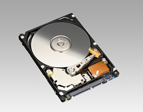
Fujitsu to Release New Energy-Efficient 500 GB 2.5" HDD Models
14:45Fujitsu Limited today announced that it has developed two new 500 GB 2.5" hard disk drive (HDD) models that feature a rotational speed of 5,400 RPM and deliver industry-leading levels of energy efficiency. The MJA2 BH series will be available from the end of December 2008, and the MJA2 CH series will be available in the first quarter of the 2009 calendar year.
With industry-leading levels of energy efficiency, the new models consume only 1.4W of power when recording data, one-third less than previous models. Moreover, these are Fujitsu's first halogen-free HDD models, making them an environmentally friendly products across their lifecycle, from deployment to disposal.
In addition, to meet information security needs for high data storage capacity applications, the MJA2 CH series is the world's first 500 GB HDD line equipped with 256-bit Advanced Encryption Standard (AES) encryption.
As corporations and government agencies have become increasingly involved in efforts to prevent global warming and promote environmental conservation, eco-friendly IT products have been at the center of attention.
To respond to these needs, Fujitsu developed two new 2.5" HDD models, the MJA2 BH and MJA2 CH, featuring industry-leading levels of power efficiency.
By increasing recording density, the new models deliver a maximum of 500 GB in storage capacity. The HDDs consume only 1.4W of power to record data, a reduction of 33% in power consumption compared to previous models. Moreover, in addition to being manufactured in compliance with the EU's RoHS Directive, which limits the use of hazardous substances, the new modes are also Fujitsu's first HDD line to be halogen-free. This will minimize the hazardous substances generated at disposal.
To prevent data leaks for customers handling sensitive information, the MJA2 CH model has a built-in encryption function. This model automatically encrypts data as it is recorded, and all data stored on the HDD can be erased instantly, in less than a second, using the advanced secure erase feature. These features prevent data leaks in the event a PC is lost or stolen and make it simple to erase data during disposal, thereby reducing customers' total cost of ownership.
With high storage capacity and low power consumption, MJA2 BH and MJA2 CH series target not only the expanding notebook PC market but also other markets such as desktop PCs.
The HDDs are the most recent offerings under Fujitsu's Green Policy Innovation program, which was unveiled in December 2007 to promote energy-efficient products and services as a way to help customers lower their ecological footprint.
Capitalizing on the vast experience and reputation for reliability that Fujitsu has accumulated through over 40 years of HDD development, these products will deliver the superior quality and environmentally friendly features that customers have come to expect from Fujitsu.
Pricing and Availability
| Series | Price | Shipment |
|---|---|---|
| MJA2 BH | Quoted per order | End of December, 2008 |
| MJA2 CH | Quoted per order | First quarter of 2009 calendar year |
Fujitsu Achieves Record-Breaking Quarter in Hard Disk Drive Shipments
14:43Fujitsu Computer Products of America, Inc., a leading supplier of innovative computer products including hard disk drives, peripherals and biometric security solutions, today announced a record-high hard disk drive (HDD) shipment of 10.5 million units in the third quarter of 2008, underscoring the company’s sustained commitment to its HDD business and its valued partners and customers. Increasing adoption of Fujitsu mobile HDDs drove record high shipments of 8.9 million units, while enterprise HDD shipments held steady at 1.6 million units, maintaining the second position in the enterprise HDD segment.
“Despite the slowing economy and challenging economic conditions, Fujitsu had a record quarter for its hard disk drive business and continued its commitment to delivering reliable, high performance and energy efficient hard drives,” said Joel Hagberg, vice president, marketing and business development, Fujitsu Computer Products of America, Inc. “Demand for our mobile drives, continues to be strong as we advance our technology to meet today’s emerging storage needs.”
Of the total HDD shipments made throughout the quarter, the 5400 RPM Serial ATA (SATA) products made up 91 percent of all mobile HDD shipments at 8.1 million units. These shipments stem from the strong, ongoing demand for high capacity, 2.5-inch drives, which are ideal for notebooks and consumer electronics applications requiring high performance and low-power consumption. In addition, Fujitsu continues to be a leader in the HDD industry delivering the first AES 256-bit Full Disk Encryption model, MHZ2 CJ series, in the third quarter of 2008.
Of the enterprise HDD shipments, 75 percent were Serial Attached SCSI (SAS) drives, indicating strong demand for mission critical server and storage system applications. Fujitsu also enjoyed an increase in shipments of its small form factor SAS drives as a result of their leadership position in the industry transition from 3.5-inch to 2.5-inch HDDs for enterprise class server and storage systems that require space-saving designs and low power consumption.
From: http://www.fujitsu.com
CONVERGENT INDUSTRIAL APPLICATIONS PROFIT FROM WIDESPREAD ADOPTION OF ANALOG DEVICES PROCESSORS
10:49The industry’s broadest portfolio of embedded and signal processing choices is what increasingly attracts industrial application developers to technologies from Analog Devices, Inc. This is especially true for the industrial control, and test and measurement designs that require performance scalability, power and cost efficiency, and connectivity to a wide variety of industry standard communications protocols. The company’s Blackfin and SHARC processor families not only meet these demands, but drive fast time-to-market with a robust ecosystem of development tools and third-party solutions for a wide variety of industrial markets.
Developers find the Blackfin processor family ideally suited for a wide range of industrial designs where a convergence of capabilities is necessary. These include multiformat audio, video, voice, and image processing; multimode baseband and packet processing; and real-time security and control processing. Recent Blackfin family product announcements highlight new features that add to an already rich variety of features and peripherals. The IEEE1588 functionality integrated into the new BF518 processor, for example, will make an immediate impact in IP-connected control and measurement systems, and the device’s PWM feature is ideal for motor control designs.
"Blackfin has delivered superior performance in our systems to allow us to optimize our power meter equipment both with regards to cost and functionality in terms of grid automation and communication", said Alexander Schenk, Head of subdivision AMIS, Siemens. "Furthermore Blackfin allows us to scale our newest generations of systems to give our customers the possibility to "smarten" their grids step by step as demanded by the EU directives and legislation."
Based in Vienna, Austria, the AMIS-Subdivision has led Siemens' development efforts to provide and introduce a seamless and complete solution with regards to smart power automation and smart power metering for utility market and energy providers.
“Blackfin processors give us the right mix of processor power, memory capacity and richness of peripherals to efficiently handle diverse tasks,” said Marco Schmid, President and CEO of Schmid Engineering. The company, using 5 networked Blackfin processors in a recent design to locate and repair rail defects, relies on reliability and scalable performance across a wide range of functions from machine control and user interfaces to complex signal processing. “The integration of a system as complex as ours was also greatly enhanced by support from leading embedded tools vendors for the Blackfin processor,” concluded Schmid.
Microsoft’s recently announced support for the Blackfin processor in its .NET Micro Framework adds the very powerful and widely adopted Visual Studio tools to the Blackfin kit for programming ‘ease of use’.
ADI’s SHARC processors provide the industry’s best floating-point performance for industrial applications where dynamic range is a key consideration. SHARC devices dominate the floating-point digital signal processing market, delivering exceptional core and memory performance complemented by outstanding I/O throughput.
"The SHARC processor is intuitive, easy to work with and highly cost-effective....definitely a slam-dunk choice,” said Bob Higgins, principal electrical engineer at Polhemus, who uses SHARC for its latest 16-sensor, 3D motion tracking system. Higgins says his team chose the SHARC processor for its high degree of math precision and accuracy, its support for IEEE- fixed and floating point math compatibility, and the way the processor’s general-purpose I/O pins simplified sensor interfacing. "The number crunching is great," said Higgins, “plus ADI's support, which includes people with years of experience, is fabulous."
From: http://www.analog.com
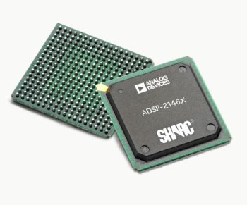
NEW SHARC® PROCESSORS PROVIDE THE INDUSTRY’S HIGHEST-PERFORMANCE FLOATING-POINT DSP
10:36Analog Devices broadened its new fourth generation SHARC® family, the industry’s highest-performance floating-point digital signal processors, by introducing a series of processors for industrial and instrumentation, automotive audio, and home theater applications. Sharing the same higher-performance design as the pro audio version of the SHARC 21469 (commercial temperature range) introduced in October, at up to 450 MHz/2700 MFLOPS these newest processors more than double the total computational performance of the previous SHARC generation. A number of key features across the SHARC 2146x lineup contribute to this impressive performance and I/O throughput, including hardware accelerators, increased on-chip SRAM, a high-speed DDR2 SDRAM external memory interface, and link ports.
Five New SHARC Processors Join the Family
The SHARC processors introduced today are: the 21469 (industrial temperature range packaging) for industrial and instrumentation; the 21469W, 21465W, and 21462W for automotive audio; and the 21467 for home theater. Like their predecessors, this newest generation of SHARC processors is based on a single-instruction multiple-data (SIMD) core that supports 32-bit fixed-point as well as 32-/40-bit floating-point arithmetic formats, making them particularly suitable for high-performance applications.
“SHARC has been the leader in floating-point digital signal processing because of its exceptional performance and a high degree of integration that yields a great price/performance benefit,” said Jerry McGuire, vice president, General Purpose DSP, Analog Devices, Inc. “With the next generation of SHARC processors, we’ve continued to listen to our customers: We’re providing the highest-performing standard floating-point DSPs and adding requested features such as integrated peripherals and accelerator engines to perform specific tasks, making more of the core available for increased processing needs.”
Like the pro-audio-optimized version that debuted last month, these new fourth-generation SHARC processors offer more than two times the 32-bit floating-point family’s performance compared with earlier SHARC offerings. One key contributor to this performance increase is the addition of hardware accelerators for widely used signal processing operations: FIR (Finite Impulse Response), IIR (Infinite Impulse Response), and FFT (Fast Fourier Transform).
Additional new features that substantially boost the performance of the SHARC 2146x include: an increase of 60 percent in on-chip SRAM up to 5Mbits and a new Variable Instruction Set Architecture (VISA) feature that allows a reduction in instruction opcode size, freeing up as much as 30 percent of memory space for application code. Furthermore, faster I/O throughput is achieved by a high-speed DDR2 SDRAM external memory interface that effectively doubles the data transfer rate. For data transfers between multiple SHARC processors, link ports provide a parallel command interface for faster data movement than is enabled by the processors’ serial peripheral interface (SPI).
Industrial and Instrumentation
Thanks to its high performance, large on-chip memory, high-speed external memory interface, and flexible peripherals -- including eight fully independent serial ports (SPORTs) -- the 21469 provides a strong value proposition for industrial and instrumentation applications that depend on SHARC processors’ real-time deterministic program execution. Designs further benefit from a thermal diode that aids in monitoring die temperature by letting developers set their own parameters with respect to frequency and voltage.
Example industrial and instrumentation applications for the SHARC 21469 include power and process control including any kind of high dynamic range data acquisition; motion control including robotics and intelligent servo drives; and test and measurement including oscilloscopes, signal generators, and signal sources.
“SHARC has delivered superior performance in our systems that sense and react to faults and transient events in the power grid,” said LiJiuhu, R&D director, Nanjing Nari-Relays Electric Co., Ltd. “For that reason, it’s great to know this new generation of the processor takes performance to the next level and gives us more room to advance our solutions.” Based in Nanjing, China, NR is a leading company in research and manufacturing of numerical protection, automation, and control systems for both HVAC and HVDC power systems.
Automotive Audio and Home Theater
To help audio developers achieve faster time to market and drive down overall system cost, the new SHARC processors targeted for automotive audio applications (21469W, 21465W, 21462W) and home theater (21467) complement their next-generation SHARC performance with certified implementations of decoders in on-chip ROM: including DTS-HD® Master Audio, Dolby® Digital Plus, Dolby TrueHD, and many more. This continues ADI’s leadership in working with intellectual property holders to implement the latest audio formats including those required by high-definition, surround-sound systems.
Additional hardware engines for Digital Transmission Content Protection (DTCP) (21465W, 21462W) and sample rate converter (SRC) (all 2146x family members) perform these specialized operations in hardware rather than software, making more core performance available for overall application processing. The SHARC 21469W, 21465W, and 21462W bring further performance acceleration to in-vehicle applications that use these processors’ integrated MediaLB interface for connecting to automotive MOST® (Media Oriented Systems Transport) networks.
Among the integrated peripherals that help reduce bill of materials (BOM) cost for end-product design on the SHARC, 21469W, 21465W, 21462W, and 21467 is the S/PDIF (Sony/Philips Digital Interface) transmitter/receiver, an industry-standard I/O interface for digital audio applications.
Pricing and Availability
The new SHARC processors will be available to sample in Q1 2009. Pricing is $31.50 in quantities of 1,000 for the ADSP-21469 at 450 MHz, while the 400 MHz ADSP-21469 lists at $28.50 for 1,000 pieces.
From: http://www.analog.com