
Archive : 6 November 2008 year
Invitrogen Launches Microarray to Study Non-Coding RNA
22:23Invitrogen Corp. (NASDAQ: IVGN), a provider of essential life science technologies for research, production and diagnostics, today announced the launch of the first high-density microarray for the profiling of non-coding RNAs. The NCode Human and Mouse non-coding RNA microarrays consist of both non-coding RNA and messenger RNA (mRNA) content on the same array. The arrays are designed by Invitrogen and then manufactured by Agilent Technologies Inc. (NYSE: A), a technology leader in communications, electronics, life sciences and chemical analysis, using the company's proprietary SurePrint technology.
Transcription, or the synthesis of RNA as directed by DNA, involves not only mRNA corresponding to the genes that are translated into proteins, but also tens of thousands of long non-protein-coding RNAs. These non-coding RNAs appear to comprise a vast hidden layer of genetic programming implicated in development and disease pathways in mammals.
"Non-coding RNA transcripts play a variety of roles in a cell, ranging from simple housekeeping to complex regulatory functions, and evidence is mounting that their expression is perturbed in many cancers," said John Mattick, Ph.D., professor of Molecular Biology at the University of Queensland, Australia. "Because their function remains largely unknown, these transcripts represent a new frontier of molecular genetic, molecular biological, physiological and cell biological research."
The NCode non-coding RNA microarrays contain sequences of RNA that do not code for proteins along with sequences of RNA corresponding to mRNAs, which are translated into proteins in a cell. The non-coding sequences were generated and subsequently validated by Professor Mattick's team at the Institute for Molecular Bioscience, and exclusively licensed by Invitrogen.
"When we talked to scientists about their interest in studying non-coding RNA, many told us they wanted a microarray that consisted of both mRNA and non-coding RNA content, which would help them elucidate the function of specific non-coding RNAs in relation to known pathways of gene expression," said Amy Butler, vice president of Gene Expression Profiling for Invitrogen. "We answered with an array-based solution, exclusive to Invitrogen, that has tens of thousands of coding and non-coding sequences which could answer multiple scientific questions with a single experiment."
Because the NCode non-coding RNA microarrays include thousands of individual sequences, they must be spotted very densely on a glass slide. To meet this density requirement, Invitrogen partnered with Agilent to use Agilent's proprietary SurePrint technology to manufacture the NCode non-coding RNA microarrays. Invitrogen will market and distribute the product.
"The precision and flexibility of Agilent's Sureprint technology enables an unmatched level of performance and quality that is essential to conduct array-based gene expression research," noted Yvonne Linney, Ph.D., Agilent vice president and general manager, Genomics. "By selecting SurePrint technology to manufacture this new array for research use, Invitrogen is ensuring the consistent performance of the NCode non-coding microarrays."
For more information, visit www.invitrogen.com/Ncode.
From: http://www.agilent.com
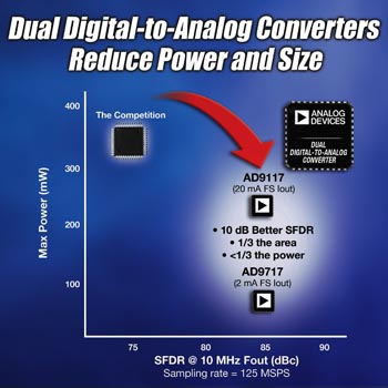
ANALOG DEVICES INTRODUCES EIGHT HIGH-SPEED, LOW-POWER DIGITAL-TO-ANALOG CONVERTERS
21:46Analog Devices, Inc. the global leader in data conversion technology, is helping electronic equipment manufacturers design more energy-efficient products with the introduction today of eight TxDAC® transmit digital-to-analog converters (DACs), each integrating two DACs on a single device. Adding to ADI’s extensive high-speed DAC portfolio, the new pin-compatible dual TxDAC converters are designed for communications, industrial, instrumentation and other demanding high-performance applications for which low power consumption and space savings yield significant cost, performance and time-to-market advantages. Dissipating only 220 mW at their maximum sample rate, the AD911x series of dual TxDAC devices consume 40 percent less power and are one-third the size of competing transmit DACs, while achieving 10 dB better SFDR (spurious-free dynamic range) performance. The AD971x series of dual TxDAC devices, with 2-mA full-scale output current, are even more energy efficient, consuming 70 percent less power than competing solutions.
“With the industry increasingly focused on efficiency and portability, design engineers are being squeezed to reduce power consumption and board space in their designs,” said David Robertson, product line director for the High Speed Signal Processing group, Analog Devices. “Whether they’re designing femtocell base stations, battery-powered instrumentation or medical applications, designers are looking for new DAC products that will help them meet their space and power budgets, without sacrificing performance.”
Low Power, Integration and Flexibility
Each new TxDAC integrates two 14-, 12-, 10- or 8-bit digital-to-analog converters with sample rates up to 125 MSPS (mega-samples-per-second). These devices allow designers to adjust the full-scale current from 1 to 4 mA or 4 to 20 mA with a single, pin-compatible architecture and common software code.
The AD971x TxDAC series features 1- to 4-mA maximum differential output current. Power dissipation at 2 mA output current is only 37 mW at 10 MSPS and 53 mW at 50 MSPS. This is one-third that of competing transmit DACs, making the new series ideal for small, limited range wireless equipment, such as picocell and femtocell base stations and battery-powered medical, industrial and instrumentation applications.
The AD911x TxDAC series has 4- to 20-mA maximum differential output current. It dissipates 40 percent less power than other devices in its class and is suited to automotive, medical, instrumentation and communications applications where channel densities must be maximized without the addition of cooling fans or where environmental considerations are driving a reduction in power consumption. The AD911x devices achieve 85-dB SFDR to 10 MHz, which is superior to other devices in its class.
Despite their small 6 mm x 6 mm package size, the new DACs are loaded with performance features, such as an internal calibrator for improved INL and DNL performance up to a 10-MHz output frequency, an internal voltage reference, independent full-scale current control, on-chip load and common-mode resistors, and a pair of auxiliary DACs that can be used for generating control voltages or for system calibration.
The new TxDAC devices offer a seamless interface to ADI’s high-performance quadrature modulators, such as the ADL5370. If a single-ended or differential-buffered voltage output is needed, then the ADA4899-1 and ADA4841-2 operational amplifiers are excellent choices, respectively. Additionally, Analog Devices’ high speed converters, such as the AD911x TxDAC family, are designed to operate seamlessly with ADI’s AD9513 clock distribution IC and new line of voltage regulators, including the ADP3334 and ADP3333.
Pricing and Availability The TxDACs are available now in volume production. The devices come in a small, 6 mm × 6 mm, Pb-free, 40-lead LFCSP (lead-frame chip-scale package). For more information, visit http://www.analog.com/pr/AD971x.Atmel Launches Low-frequency RF IDIC with Megapads for Direct Coil Bonding
21:44Atmel® Corporation announced today the availability of the 363-bit read/write transponder IDIC® ATA5577M2. This device features large gold-bumped pads for direct bonding of the copper antenna coil. With integrated LC-tank-capacitors trimmed to a +/- 3% tolerance, the antenna coil is the only external component needed for a complete trimmed tag system, thus providing significant cost savings.
The IDIC provides a manufacturer-programmed unique ID which is vital to guaranteeing access to secured areas. The unique ID also enables the traceability of the product, thus preventing easy cloning or counterfeiting of the tag IC. The unique ID and extended read/write distance have been optimized for next-generation access control applications including hotel rooms, engineering departments, offices, time recording systems, parking lots and customer loyalty and membership cards. In addition, the new device operates according to ISO 11784 and ISO 11785 (FDX-B) standards, making it well-suited for animal identification and waste management applications.
Since the ATA5577 is a low frequency (LF) device, it can be used worldwide. It is not sensitive to rugged environments and can also be used under conditions that normally complicate the application of RFID devices such as water, metal, or dirt; out-of-sight; or being worn on the body.
Including the optional trimmed 250- or 330-pF on-chip capacitors, the ATA5577M2 is only 1 millimeter in width, which allows the chip to be used in almost any transponder package including glass transponders for animal identification.
The device's new architecture enables outstanding read/write performance with differing types of coils, readers, and parameters which is especially important for animal and waste management applications. A special register maximizes the overall read and write distance for each application environment. Thanks to a dedicated write procedure (downlink, reader-to-tag), the write distance has been increased to industry leading distances. This increased write distance is especially beneficial for applications in difficult environments.
Availability and Pricing
Samples are available now as sawn wafer on foil or die in waffle pack. Pricing for the ATA5577M2 as sawn-wafer shipment with quantities of 15k pieces starts at US$ 0.49. To support the system designer, Atmel provides the evaluation kit ATA2270-EK1. This is based on Atmel's LF-RFID reader chip U2270B and the AVR® microcontroller ATmega128. The kit includes all C-routines and PCB layout data in Gerber format. In addition, several tag samples are supplied with the kit for easy system implementation. In addition, a PC-based graphical user interface is also available. The ATA5577M2 can replace and is backward compatible with Atmel's well-known existing LF devices in several applications.
From: http://www.atmel.com
Atmel Launches a New AVR Microcontroller for Smart Card Reader Applications
21:42Atmel® Corporation announced today the introduction of its new AVR® microcontroller designed for smart card reader applications. Based on the AVR 8-/16-bit RISC core allowing single cycle instruction execution, the AT90SCR100 embeds 4 Kbytes of EEPROM for data, 4 Kbytes of SRAM and 64 Kbytes of programmable FLASH providing all the flexibility required for fast software upgrade and customization reducing significantly time to market and development costs both during development phase and product life.
The AT90SCR100 offers a comprehensive set of interfaces such as ISO7816 (Class A,B,C supported), USB full Speed 2.0 device and host, USART and TWI to address any applications that interface to synchronous, asynchronous and USB smart cards. In addition, a SPI serial interface plus a dedicated High Speed SPI interface (up to 20Mbps at 20MHz) have been implemented. Respectively combined with an RF front end and/or with a fingerprint sensor, the AT90SCR100 is ideally suited to contactless and/or Biometric reader applications. With its 38 GPIOs in its high pin count configuration (64 pin package), it can also address all USB Keyboards integrating the smart card reader functionality.
Thanks to its integrated hardware AES 128/256 bits engine that leaves complete availability of the Flash for the end user application, the AT90SCR100 is the first smart card reader microcontroller on the market to offer cryptographic capability. Consequently, communication through secure channels can be performed without calling for any CPU resource during the ciphering operations.
"Migrating to the powerful proprietary AVR architecture will reinforce our market leader position in the smart card reader microcontroller market," stated Jean-Charles Lesage, Atmel's Smart Card Reader ICs Marketing Manager. "The AT90SCR100 is the first product of a new family that anticipates the increasing growth of smart card reader technology. With over 7 billion smart cards in the field by the end of 2009 and the promising future of 'SmartObjects' such as Notebook, Ultra Mobile Devices in various form factors, needs for many types of readers will become a reality. Thanks to its new AT90SCR family, Atmel is already prepared to face this exciting challenge."
Development Tools – The AT90SCR100 also takes benefit from the free AVR Studio® and AVR JTAGICE mkII supporting all AVR devices and development tools, including starter kits, evaluation kits and reference designs. A dedicated evaluation kit providing access to all communication interfaces in combination with First Software Layers library will be available in January 2009.
Availability and Pricing
Samples for the AT90SCR100 are available now. Packages are available in 32-pin QFN, 64-pin QFN and 64-pin QFP. Volume production will start in May 2009. Prices start at US$ 3.00 for the 64 pin count version and at US$ 1.90 for the 32 pin package in 10,000 quantities.
From: http://www.atmel.com
Atmel Extends its secureAVR Product Family for Banking Card Applications
21:40Atmel® Corporation announced today the introduction of its new AT90SC16018RU secure microcontroller to extend its product offering for banking card applications. The large ROM memory in the device allows customers to implement sophisticated applications such as CPA (Common Platform Application) for the EMV banking, SDA (Static Data Authentication) market and makes this chip perfectly suited for cost sensitive applications such as medium end contact banking cards.
Based on Atmel's optimized 8-/16-bit RISC secureAVR® CPU architecture, the AT90SC16018RU features on-chip high density, well-tailored memories: 16 Kbytes of EEPROM, 160 Kbytes of user-ROM, and 4 Kbytes of RAM. This product has been designed to meet the security standards of Common Criteria EAL5+ and EMVCo. It shares the same common features with Atmel's secureAVR family including dedicated hardware for protection against SPA/DPA/SEMA/DEMA attacks as well as advanced protection against physical attacks.
Herve Roche, Atmel's Banking and Telecom Marketing Manager stated, "The introduction of this new device perfectly completes Atmel product portfolio and reinforces Atmel's commitment to serve all the contact based products for banking market. We strongly believe that this new product will help our customers to develop innovative Operating Systems and application codes to serve in long term a cost sensitive market requiring more and more security."
Availability and Pricing
AT90SC16018RU samples are available now. Volume production will start in Q1 2009. Prices start at US$ 0.60 for 10k units.
From: http://www.atmel.com
Tektronix Provides Choice for Serial Data Link Analysis
21:38Tektronix, Inc., a leading worldwide provider of test, measurement and monitoring instrumentation, announced new Serial Data Link Analysis (SDLA) Software for the DSA70000 real-time oscilloscope series to fully test high-speed serial data designs such as SATA 6 Gb/s, SuperSpeed USB, 6 Gb/s SAS and PCI-Express 3.0, from the transmitter through the receiver. The new SDLA software builds on the Tektronix history of providing link analysis and S-parameter tools for precise silicon designs with the DSA8200 sampling oscilloscopes. With SDLA software, engineers can now utilize a real-time oscilloscope to develop compliant high-speed serial designs on systems that operate as high as 8 Gb/sec.
For high-speed serial data technologies, the interactions between the transmitter, possible test fixture and the transmission line are so complex that analysis needs to include all possible signal impairment conditions along the path. If done manually, complete link analysis on high-speed serial data can be time-consuming and error-prone. The Tektronix SDLA Essentials software provides channel emulation, transmitter pre- and de-emphasis, test fixture de-embedding, time and frequency domain plots to aid debug. Additionally, the package provides a seamless interface with DPOJET, a comprehensive package for jitter and BER analysis.
An SDLA Advanced option adds Feed Forward Equalization (FFE) and Decision Feedback Equalization (DFE) with three modes of adaptation to emulate the waveform at the receiver. Through tight integration with DPOJET, digital designers gain simultaneous jitter and eye diagram feedback as they introduce different parameters to the link, from channel effects to equalization approaches. The software can eliminate the causes or adjust the impact of signal distortion and transmission failure across serial links.
"Faster data rates are narrowing serial data system timing margins,” said Ian Valentine, general manager, Technology Solutions Group, Tektronix. “With the introduction of Serial Data Link Analysis software for the DSA70000 real-time oscilloscopes, engineers can evaluate all characteristics impacting a serial data link, from transmitter pre-emphasis through the transmission medium to equalization on the receiver. The SDLA and DPOJET packages for the DSA70000 oscilloscopes substantially improve jitter and timing analysis of high-speed serial designs.”
Complete Link Impairment Compensation
Equalization is a broad term for several techniques of manipulating the signal shape in order to overcome frequency dependent loss of the channel. This loss changes the shape of the NRZ data signal at the receiver from the desired square-wave to severely distorted, closed eye waveform. SDLA software provides FFE and DFE equalization methods on the receiver side, and the generation and measurement of pre-emphasis and de-emphasis on the transmitter side.
SDLA also provides channel emulation. Through emulation, engineers are able to see waveform impairments due to channel transmission loss. For example, the testing specification for emerging Serial Attached SCSI (SAS) 6Gb/s standard requires that engineers de-embed the test channel and enable emulation of the test pattern to include a 3 tap DFE for full system evaluation. This measurement capability is now enabled by the Tektronix SDLA Advanced package. When using DPOJET in combination, SAS measurements are pre-configured and automated.
Price & Availability
SDLA Essentials and SDLA Advanced are available for order and delivery. U.S. MSRP for SDLA Essentials is $3,000 and $7,000 for SDLA Advanced.
From: http://www2.tek.com
Vishay Releases New ECL Series of SMD Aluminum Capacitors With Z as Low as 90 mΩ, High Capacitance Values up to 1500 µF, and High Ripple Currents to 670 mA
21:33Vishay Intertechnology, Inc. (NYSE: VSH) today announced the release of a new series of surface-mount aluminum capacitors that offers high-temperature operation +105 °C, low impedance values, and high capacitances and ripple currents.
Designed for surface mounting on high-density PCBs, the new ECL series of polarized aluminum electrolytic capacitors features a non-solid, self-healing electrolyte. For high-temperature operation, a heat-resistant pad and molded base plate provide additional stability and protection.
Available in six case sizes, ranging from 6.3 mm by 5.8 mm to the larger 12.5 mm by 13.5 mm (width by height), the devices are optimized for inverter circuits and filtering, smoothing, and buffering applications in industrial systems and consumer electronics, such as audio equipment, flashes, and computers.
For enhanced performance and reliability, the capacitors offer a very low impedance Z down to 90 mΩ at 100 kHz, a high rated ripple current of 670 mA at +105 °C, and a capacitance range from 10 µF to 1500 µF over a voltage range of 6.3 V to 100 V.
Specified according to IEC 60384-4/EN 130300, the ECL devices feature a long life of 2000 hours at +105 °C. Supplied in blister tape-on-reel packaging, the RoHS-compliant capacitors are compatible with reflow soldering and automatic insertion machines.
Samples and production quantities of the new ECL series are available now.
Vishay Intertechnology, Inc., a Fortune 1,000 Company listed on the NYSE (VSH), is one of the world's largest manufacturers of discrete semiconductors (diodes, rectifiers, transistors, and optoelectronics and selected ICs) and passive electronic components (resistors, capacitors, inductors, sensors, and transducers). These components are used in virtually all types of electronic devices and equipment, in the industrial, computing, automotive, consumer, telecommunications, military, aerospace, and medical markets. Its product innovations, successful acquisition strategy, and ability to provide "one-stop shop" service have made Vishay a global industry leader. Vishay can be found on the Internet at http://www.vishay.com.
From: http://www.vishay.com
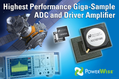
National Semiconductor Introduces Industry's Highest-Performance, 10-Bit, 1 GSPS Signal Path Solution
21:26National Semiconductor Corp. today introduced a 2.5 GHz fully differential amplifier and a 10-bit, 2 Giga-sample per second (GSPS) single/1 GSPS dual analog-to-digital converter (ADC) that deliver unequaled dynamic system-level performance and low power for wideband applications. These combined signal path products are well-suited for ground-based radar, data acquisition systems, point-to-point base stations and next-generation set-top boxes.
At a frequency of 248 MHz, the ADC10D1000 provides the industry’s highest spurious-free dynamic range (SFDR) performance of 66 decibels relative to carrier (dBc) and 9.1 effective number of bits (ENOB). Running off a single supply voltage, the ADC10D1000 achieves this unparalleled level of performance while consuming 33 percent less total power (2.8W) than comparable ADCs. The 2.5 GHz LMH6554 wideband, fully differential amplifier drives the 10-bit ADC10D1000, providing best-in-class 0.1 dB gain flatness up to 800 MHz, SFDR of 72 dBc at 250 MHz and leading low-input voltage noise performance of 0.9 nV/sqrt Hz.
These devices feature power-to-performance metrics that position them among National’s PowerWise® family of energy-efficient products. The ADC10D1000 yields 2.52 picojoules (pJ) per conversion, while the LMH6554 consumes 21 uA per MHz.
Highest-Performance, Lowest-Power Giga-Sample ADC
The ADC10D1000’s industry-best SFDR and ENOB allow it to maintain excellent performance through the first, second and third Nyquist zones. This new performance level enables digitization of wide swaths of bandwidth in applications that have previously had to use narrowband ADCs to achieve high-resolution sampling. For example, high-resolution radar systems now can use fewer parallel channels to digitize the same bandwidth, enabling significantly reduced board size and power dissipation. The ADC10D1000’s extremely low 2.8W power consumption also enables system design without heat sinks over the -40 degrees C to 85 degrees C industrial temperature range, which saves space and weight.
The ADC10D1000 digitizes a pair of analog input signals at sampling rates up to 1 GSPS, or a single analog input signal at speeds up to 2 GSPS. Additional features include AutoSync for multi-chip synchronization and programmable gain and offset adjustment for each channel. The internal track-and-hold amplifier and the extended self-calibration scheme enable a very flat response of all dynamic parameters beyond Nyquist, while providing an exceptionally low 10 (-18) code error rate. The ADC10D1000 is supplied in a leaded or lead-free, 292-ball, thermally enhanced BGA package.
Highest-Performance Fully Differential Gigahertz Amplifier
The LMH6554 is a 2.5 GHz fully differential amplifier that provides exceptional signal fidelity for driving 8- to 16-bit high-speed ADCs. The device’s low impedance differential output is designed to drive ADC inputs and any intermediate filter stage. The LMH6554 delivers 16-bit linearity up to 75 MHz when driving 2V peak-to-peak into loads as low as 200-Ohms. With external gain set resistors and integrated common-mode feedback, the LMH6554 can be used in differential-to-differential or single-ended-to-differential configurations. The amplifier provides large signal bandwidth up to 1.8 GHz, 8 dB noise figure and a slew rate of 6200 V/us.
The LMH6554 is manufactured on National’s new CBC8 silicon germanium (SiGe) complementary bipolar-CMOS process technology. Among the most advanced analog processes in the industry today, the CBC8 process features a unique, monolithic, combination of SiGe NPN and PNP transistors, as well as low power CMOS transistors that enable exceptional speed, linearity, circuit density, low power and low noise for demanding high speed analog applications. The LMH6554 operates over the extended temperature range of -40 degrees C to 125 degrees C and is supplied in a space-saving, thermally enhanced, 14-pin flip-chip on lead (FCOL) package.
Reference Board and Tools Accelerate Signal Path Development
A reference board that includes the ADC10D1000, LMX2531 clock source and a field-programmable gate array (FPGA) interfaces directly with National’s new WaveVision 5 software to simplify the evaluation process. The WaveVision 5 system is an easy-to-use analysis tool, designed to help users evaluate National’s signal path products. For example, the ADC10D1000 can be teamed with the LMH6554 amplifier as well as LMX2531 single-chip phase-locked loop (PLL) and voltage-controlled oscillator (VCO) or one of National’s LMK04000 family of clock jitter cleaners to form a complete signal path solution.
Pricing and Availability
The ADC10D1000 and LMH6554 are sampling now, with production quantities scheduled for first quarter 2009. For more information on the ADC10D1000’s pricing, samples and reference boards, visit www.national.com/pf/DC/ADC10D1000.html. The LMH6554 is priced at $4.50 in 1,000-unit quantities. For more information, or to order samples, visit www.national.com/pf/LM/LMH6554.html.
From: http://www.national.com
Freescale helps reduce cost and complexity of instrument clusters for entry-level vehicles
21:23Freescale Semiconductor has introduced a cost-effective family of 16-bit microcontrollers (MCUs) designed for electromechanical instrument clusters used in entry-level vehicles – a rapidly growing segment of the automotive industry. The latest addition to Freescale’s expanding 16-bit MCU portfolio, the new S12HY family combines affordable 16-bit performance with the optimal on-chip features for cost-sensitive dashboard applications in emerging automotive markets.
The S12HY MCUs provide exactly the right amount of on-chip integration to enable the migration from mechanical solutions still used in emerging markets to modern electromechanical instrument clusters. The devices’ high degree of on-chip integration helps reduce system costs by minimizing the need for separate components. An integrated liquid crystal display (LCD) driver supports up to 160 segments for LCD-based instrument clusters. The devices’ on-chip stepper motor controller can drive up to four gauges, providing precise step-by-step control for speedometers, tachometers and other analog gauges. The MCUs also feature a controller area network (CAN) module that simplifies data communications between the engine and dashboard cluster.
The S12HY devices offer up to 64 KB of on-chip flash memory for non-volatile program storage, as well as 4 KB of flash memory for data storage with error correction code (ECC) technology. Freescale’s flash-based MCUs are priced to compete with hard-coded read-only-memory (ROM) devices, while offering much greater flexibility. With a flash-based solution, developers can design a wide range of instrument clusters based on one reprogrammable16-bit MCU product. This ease of dashboard development results in reduced system cost, simpler manufacturing logistics and faster time to market.
“We have tailored the S12HY MCUs to meet the ‘sweet spot’ of the entry-level automotive market in rapidly emerging markets, such as China and India,” said Kevin Klein, global automotive MCU marketing manager at Freescale. “Why should automotive developers have to choose costlier solutions containing more features than they need? Our S12HY MCUs offer an optimal set of on-chip features and package and memory options that developers need for cost-sensitive dashboard designs – no more and no less than what’s required to design a basic electronic instrument cluster.”
In addition to offering scalable 16-bit performance and optimal features, the S12HY family is available in two LQFP package options (from 64 to 100 pins) that are ideal for cost- and space-constrained cluster designs. The family also offers a smooth migration path to more powerful S12X devices, enabling developers to scale their designs as their flash memory and performance requirements increase. The S12 MCU family is the most widely adopted 16-bit architecture in the automotive market. Freescale has shipped approximately 400 million 16-bit S12 and S12X MCUs to date, and S12-based devices continue to ship at a rate of more than 100 million units per year.
Freescale offers the broadest portfolio of MCUs for instrument clusters, supporting simple to complex designs, from mopeds to luxury cars. In addition to the 16-bit S12 family, Freescale also offers higher-performance 32-bit options based on Power Architecture™ technology, such as the MPC560xS MCUs and MPC5121e multicore processor.
Driving faster time to market
To help developers speed time to market, the S12HY family leverages the extensive suite of hardware and software development tools available today for the S12 and S12X families. Freescale plans to offer a cost-effective S12HY family demonstration board (DEMO9S12HY64) in Q1 2009. The CodeWarrior® Development Tool Suite and a range of third-party development software support also enable rapid application development.
S12HY MCU key features
- HCS12 CPU core with 32 MHz bus
- On-chip memory
- Up to 64 KB flash with ECC
- 4 KB data flash with ECC
- 4 KB SRAM
- Integrated LCD driver, configurable up to 40 x 4 (160 segments total)
- Stepper motor controller with up to four gauge drivers
- Multi-scalable controller area network (MSCAN) module (supporting CAN 2.0A/B)
- Phase locked loop (PLL) frequency multiplier with internal filter
- Two timer modules with I/O channels that provide a range of 16-bit input capture, output compare, counter and pulse accumulator functions
- Pulse width modulation (PWM) module with up to eight 8-bit channels
- Up to 8-channel, 10-bit resolution analog-to-digital converter
- Serial peripheral interface (SPI) module
- Serial communication interface (SCI) module supporting LIN 2.0, 2.1 and SAE J2602 communications
- Inter-integrated circuit (I2C) module
- On-chip voltage regulator (VREG) for regulation of input supply and internal voltages
- 64-pin and 100-pin LQFP
Pricing and availability
Freescale plans to offer samples of the S12HY MCUs to selected customers in December 2008. For pricing information, contact local Freescale sales representatives. For more information about Freescale’s S12 and S12HY MCU families, visit www.freescale.com/files/pr/automotive .
From: http://freescale.com
Freescale and Samsung Electronics announce collaboration on LED display technology
20:53Freescale Semiconductor and Samsung Electronics, a world leader in display technology, have announced their collaboration to address the burgeoning market for energy-saving and environmentally friendly light-emitting diodes (LEDs).
“Freescale’s LED backlight driver technology is the industry’s most compact and integrated solution,” said Arman Naghavi, vice president and general manager of Freescale’s Analog, Mixed-Signal and Power Division. “Our collaboration with Samsung on LED backlighting – clearly a disruptive technology – will help spur further innovation and growth in the LCD market.”
Freescale began sampling its LED display technology to Samsung in December 2007. In September 2008, Freescale introduced the first LED backlight product in its portfolio of standard power management ICs. The white LED driver IC is designed for control of LED backlights in TVs, as well as in flat-panel monitors.
Since 2007, Samsung has successfully launched award-winning products featuring its ultra high-contrast active control LED backlight technology.
According to IMS Research, the market for semiconductors used in backlighting applications, including LED driver ICs, is expected to grow from $1.1 billion (USD) in 2008 to $2.0 billion in 2012.
“We expect the market for LED backlighting in notebooks, monitors and TVs to grow strongly,” said Jamie Fox, a market research analyst for IMS Research. “In notebooks in particular, rapid growth is widely expected from 2008 to 2010.”
Freescale plans to announce additional LED backlighting solutions for LCD TVs, monitors and notebooks in the first half of next year. Also in 2009, the company intends to pursue the automotive, commercial and residential LED lighting markets, which are expected to eventually dwarf the LCD TV market.
Energy-efficient, mercury-free
LED technology offers many advantages over conventional cold-cathode fluorescent lamp (CCFL) lighting systems, which are widely used in conventional LCD displays. Conventional LCD TVs without LED backlight technology are major energy consumers within households. LED backlights with local dimming can help reduce power consumption by up to 60 percent and can enable manufacturers to adopt thinner, lighter form factors.
LED backlighting also enhances the user viewing experience, offers more flexible backlight architectures and enables thinner display designs. Additional benefits of LED backlighting over conventional CCFL technology include higher efficiency (more light at a given power), reduced power consumption, enhanced durability and up to 100 times better contrast ratios for clearer definition on screen.
LED technology is free from mercury, a substance known to be toxic to humans. Mercury is a key material in CCFL lighting systems, which are used in 99 percent of existing LCD TV displays. In Europe, the European Directive on the Restriction of Use of Certain Hazardous Substances in Electronic (RoHS) has mandated that manufacturers must move to mercury-free solutions.
About Freescale Semiconductor
Freescale Semiconductor is a global leader in the design and manufacture of embedded semiconductors for the automotive, consumer, industrial, networking and wireless markets. The privately held company is based in Austin, Texas, and has design, research and development, manufacturing or sales operations in more than 30 countries. Freescale is one of the world's largest semiconductor companies with 2007 sales of $5.7 billion (USD). www.freescale.com.
From: http://freescale.com
Freescale squeezes cost, power and complexity out of liquid crystal displays
20:51Liquid crystal displays (LCDs) are proliferating in an ever-growing array of consumer and industrial products. To help meet the demand for efficient, affordable LCDs, Freescale Semiconductor has introduced three 8-bit microcontroller (MCU) families designed to reduce system cost and power in LCD-based embedded applications.
The new Freescale LCD MCUs include the S08LL, RS08LA and RS08LE families. The L family devices offer industry-leading LCD capabilities and ultra-low-power options at affordable price points. The 8-bit MCUs are designed to address a wide range of cost- and power-sensitive LCD-based designs, from battery-backed handheld devices to wireless systems. Target applications include thermostats, meters, timers, security systems, rice cookers, coffee machines and other small consumer appliances.
L family MCUs are also ideally suited for personal diagnostic and portable health care products, such as glucose meters and pulse oximeters, which require low power operation and advanced display capabilities. The S08LL family is ideal for these applications due to its exceptional standby power consumption and multiplexed LCD driver functionality, which enables smaller designs with higher segment count.
Featuring an integrated LCD driver, L family MCUs eliminate the need for separate display driver ICs for both standard 3V and 5V LCD glass applications. The on-chip LCD drivers support up to eight backplanes, enabling developers to drive more segments with fewer pins and thus reduce system cost and design complexity. The L family supports an LCD blink mode that operates without waking up the controller core, which helps reduce overall power consumption.
“Freescale’s L family MCUs widen the range of cost-effective, ultra-low-power solutions within Freescale’s extensive LCD MCU portfolio,” said Aiden Mitchell, director of industrial and multi-market microcontrollers at Freescale. “Freescale offers the right choice of 8-bit devices for designers of battery-backed and wireless systems that require LCD support. L family MCUs provide many options for LCD segment drivers, package sizes and integrated features, giving developers greater design flexibility.”
S08LL family
The MC9S08LL16/8 devices combine an integrated LCD driver with best-in-class, ultra-low-power performance for embedded applications with LCD screens. The S08LL devices are designed to enhance portable performance, extend battery life and improve energy efficiency for a wide range of battery-operated applications and low-power devices. The S08LL family’s internally regulated voltage capability enables software contrast control, which reduces the need for extra components and extends temperature and operating voltage ranges.
Using Freescale's ultra-low-power platform, along with an LCD peripheral optimized for low power, the LL16 has achieved best-in-class standby power consumption. The LL16 supports a wide range of operation modes that can allow as low as 1.3 microamps to 6.1 microamps when driving LCD displays.
Additional S08LL device features include:
- Two ultra-low-power stop modes
- New low-power run and wait modes
- Six microsecond wake-up time
- Ultra-low-power oscillator
- Configurable 8 x 24 or 4 x 28 segment display
- Internal charge pump
- Software selectable frontplane and backplane
RS08LA and RS08LE families
The cost-effective MC9RS08LA8 and MC9RS08LE4 families are based on Freescale’s RS08 core and are intended for small appliances, medical monitoring equipment and other low-power industrial applications. The RS08LA family features Freescale’s first entry-level LCD MCUs in the sub-$1 (USD) price range, targeting cost-sensitive LCD applications. The devices are designed to help reduce the cost of existing LCD-based products and enable developers to add basic LCD functionality to applications.
The RS08LE family provides an ultra-affordable 8-bit migration path for LCD-based products currently using 4-bit MCUs that cannot meet the performance requirements of today’s embedded applications. Offering the industry’s lowest pin count LCD devices (28-pin SOIC package), the RS08LE family is capable of driving 112 LCD segments and can be used to replace less powerful 4-bit LCD drivers.
Key features for the RS08LA and RS08LE families include:
- HCS08 instruction set with added BGND instruction
- Configurable displays
- 8 x 21 or 4 x 25 (LA8)
- 8 x 14 or 4 x 18 (LE4)
- Power-saving ability to drive display while CPU sleeps
- Internal charge pump (LA8 only)
- Software-selectable frontplane and backplane
Pin and software compatibility
Freescale’s broad portfolio of software-configurable LCD devices offers pin compatibility options and shares peripherals to enhance design flexibility. Pin compatibility between the S08LL and RS08LA families enables scalability for end applications with the option to use the S08 core with the LL family or the RS08 core with the LA family. This compatibility provides a migration path to evaluate different performance options. Because the S08 and RS08 devices share the same LCD peripheral, developers can create software applications that are easily portable across the families.
LCD design made easy
Freescale L family MCUs are backed by a comprehensive ecosystem of development tools, reference designs, application notes, software examples and Web casts. The L family devices are supported by a complimentary version of CodeWarrior® Development Studio for Microcontrollers v6.2, an integrated tool suite that supports software development for Freescale’s 8-bit or 32-bit MCUs. Designers can further accelerate application development with the help of the Processor Expert™ tool, an award-winning rapid application development tool in the CodeWarrior tool suite.
To help developers explore the features and capabilities of the L family devices, Freescale offers the DEMO9S08LL16, DEMO9RS08LA8 and DEMO9RS08LE4 evaluation systems.
Pricing and availability
The L family devices are sampling now. Suggested resale prices (USD) in 10,000-piece quantities start at 90 cents for the RS08LE4; 99 cents for the RS08LA8 and $2.05 for the S08LL16. The DEMO9RS08LE4 and DEMO9RS08LA8 kits are available at a suggested resale price of $59 (USD) each. The DEMO9S08LL16 is available at a suggested resale price of $69.
For more information about Freescale’s L family MCUs, visit www.freescale.com/files/pr/lcd.html .
From: http://freescale.com
Freescale sensor controller adds smart touch to portable electronic products
20:49Touch sensors have become increasingly popular as more consumer, industrial and automotive designs include touch panels to provide simpler, more reliable user interfaces. Freescale Semiconductor, a leading designer and manufacturer of sensors, is meeting the demand for touch-sensitive control with the introduction of an ultra-low-power touch controller for two- and three-pad touch-sensing applications.
Freescale's MPR031 proximity capacitive touch sensor controller is designed to simplify the development of a wide range of touch-sensing applications, such as appliance controls, games, patient monitoring systems, remote controls, PC peripherals, webcams, vehicle and garage key fobs, dimmer switches and security systems. These compact, energy-efficient sensor controllers are especially well-suited for power-sensitive mobile electronics devices including mobile phones, multimedia players and audio controls for Bluetooth® handsets.
The MPR031 sensor can serve a wide range of applications that need to activate up to three touch pads. For example, the sensors can be used in an alarm system to replace a mechanical switch or push button. End users can simply touch an indicated command on the touch panel, and the alarm sounds or deactivates depending on the requested function. Using the MPR031 sensor to replace mechanical pushbuttons on portable electronic devices enables interface design innovations, such as the ability to enlarge the LCD display for portrait or landscape orientation placement options.
“Advances in touch sensor technology are making sensor-driven interfaces easier to implement in mobile electronics devices as well more intuitive and simpler for end users to operate,” said Demetre Kondylis, vice president and general manager of Freescale’s Sensor & Actuator Solutions Division. “Freescale’s latest touch sensor controller offers an elegant, cost-effective and reliable alternative to mechanical interfaces, which contain moving parts that are subject to wear and tear.”
Touch sensing technology is increasingly popular in consumer, industrial and automotive applications because it:
- Enables the elimination of mechanical buttons and sliders
- Provides an intuitive, easy-to-use “fingertip control” interface
- Enhances reliability by eliminating mechanical wear and tear
- Provides greater flexibility for product designers
- Reduces overall system costs
Advanced touch sensor controller portfolio
The MPR031 touch sensor controller is a CMOS-based, register-driven state machine designed to deliver exceptional system-level intelligence. The device’s on-chip tri-level filtering technology enables configurable electromagnetic interference (EMI) rejection. Proven CMOS technology helps to protect against electrostatic discharge (ESD), which can cause system-wide damage and interruption of service. Freescale’s state machine and CMOS technology also enables low operating voltage and current, resulting in low-power benefits for mobile device applications. The voltage operation range is 1.71 V to 2.75 V, which is ideal for small low-power electronics products.
The MPR031 device supports communication via the inter-integrated circuit protocol (I2C). Offering exceptional sensitivity and a specialized feature set, the sensor controllers can accommodate a wide range of system implementations. To simplify the design of touch-based applications, the sensor controllers can be used as drop-in replacements for mechanical devices or switches.
For applications that require more than three touch sensor-based buttons, Freescale also offers the MPR032 controller. The MPR032 features a secondary I2C address, which enables developers to use two of these devices in the same system.
MPR031 controller features
- Eight microamp average supply current
- Four microamp maximum shutdown current
- Compact 2 mm x 2 mm x 0.65 mm 8-lead UDFN package
- Supports up to three touch pads
- Touch sensing solution requires only one external component
- Intelligent touch detection capability
- 1.71 V to 2.75 V operation
- Threshold based detection with hysteresis
- I2C interface, with optional IRQ
- Multiple devices in a system support up to six electrodes
- -40 degrees C to +85 degrees C operating temperature range
Pricing and availability
The suggested resale price for the MPR031 touch sensor controller in 10,000-piece quantities is 61 cents (USD).
Freescale offers several kits to help reduce implementation development cycle time. The KITMPR031EVM is available at a suggested resale price of $99 (USD) each. The DEMMOMPR031EVM is available at a suggested resale price of $25 (USD) each.
For more information about Freescale’s proximity touch sensor solutions, visit www.freescale.com/files/pr/proximity.html .
From: http://freescale.com
Freescale DSP sets new performance levels to speed deployment of LTE and other next generation wireless standards
20:30Freescale Semiconductor introduces the MSC8156 processor − a six-core device based on new SC3850 StarCore DSP core technology and designed to dramatically advance the capabilities of wireless broadband base station equipment.
The MSC8156 is one of the industry’s first DSPs based on 45-nm process technology, endowing the part with performance, energy efficiency and form factor advantages. It delivers the flexibility, integration and affordability required for mainstream, near-term deployment of networks based on LTE and other next-generation wireless standards.
“Freescale’s ongoing investment in advanced networking technologies enables our customers to deliver richer, seamless and more compelling wireless experiences,” said Lisa Su, senior vice president and general manager of Freescale’s Networking & Multimedia Group. “The MSC8156 DSP offers the performance that OEMs and telecom carriers need to speed delivery of LTE and other next-generation wireless services.”
The MSC8156 is a single processor that replaces multiple discrete parts required by other solutions. When deployed in base station applications, the device is designed to deliver two times the performance of Freescale’s MSC8144 offering, which was previously the industry’s highest performing programmable DSP.
The exceptional performance of the MSC8156 supports the high data rates specified by the latest OFDMA standards and enables the high throughput and low latency requirements of next-generation base stations. The MSC8156, tuned for OFDMA-based systems providing up to five times greater spectral efficiency than many advanced HSPA networks, enables optimal economics for operators and opens the door to entirely new categories of end-user services.
"To meet growing demand for advanced 3G and 4G services, wireless infrastructure equipment manufacturers increasingly require silicon that offers exceptional performance and flexibility,” said Will Strauss, president of analyst firm Forward Concepts. “With the multicore MSC8156 DSP, Freescale has again demonstrated its ability to offer the advanced DSP technologies that its customers require. The MSC8156 is a landmark DSP that should significantly advance next-generation wireless infrastructure equipment.”
Acceleration technology adds flexibility and reduces cost
The MSC8156 DSP’s onboard Multi-Accelerator Platform Engine technology for baseband, called MAPLE-B, works in concert with the six fully programmable DSP cores to support the 3G-LTE, TDD-LTE, TD-SCDMA and WiMAX standards, as well as the symbol rate functionality of HSPA and HSPA+. Delivering multi-standard capabilities on a single platform eliminates the need to redesign hardware for different base station standards, so the device is scalable across macro-, micro- and pico-base station form factors. MAPLE-B includes Turbo, Viterbi, FFT and DFT processing engines and two configurable RISC engines, which can be reprogrammed in the future to accommodate updates.
Introducing StarCore SC3850 core technology
SC3850 core technology is Freescale’s newest generation of StarCore DSP cores. Key enhancements to the previous generation include a 2X increase in DSP multiplication capacity, significantly higher compiled code performance and an improved memory hierarchy. Micro-architectural improvements and new instructions enable the core to accelerate control functions, memory management and DSP code performance.
Development tools and software
Freescale offers a full set of development tools and enablement software for the MSC8156 device. The CodeWarrior™ Integrated Development Environment (IDE) leverages Eclipse™ technology to provide a highly comprehensive multicore development environment. It includes: C & C++ optimizing compilers, a source level debugger, core and device simulators, software analysis plug-ins for profiling and program/data trace, and the royalty-free SmartDSP operating system delivered with optimized device drivers. Development boards are available to enable software development along with a set of reference software components for 3G-LTE and other key algorithms.
Pricing and availability
Freescale plans to sample the MSC8156 to alpha customers during the first quarter of 2009. It is offered in a 783-pin FC-PBGA package. The company plans to offer the device in two versions, based on different core speeds of 800 Mhz and 1Ghz. Pricing is expected to start at $192 for 10K volumes.
From: http://freescale.com