
Archive : 14 November 2008 year
Tektronix Opens U.S. Serial Testing Technology Center
17:57Tektronix, Inc., a leading, worldwide provider of test, measurement and monitoring instrumentation, announced the opening of a serial test and measurement center in Santa Clara, California. The Santa Clara facility is one of five centers now open around the world. Each is equipped with state-of-the-art test and measurement technology. The Santa Clara Technology Center will provide a venue in Silicon Valley for demonstrations of the latest high-speed serial data test technology and methodologies. Additionally, firms can obtain consultation and assistance with testing their serial data designs.
Design engineers developing new high speed serial technologies such as Serial ATA Revision 3.0, PCI Express 2.0 and PCI Express 3.0, SuperSpeed USB, HDMI CTS1.3, and DisplayPort 1.1a, need to process large amounts of data with greater signaling complexities. Testing new devices employing these technologies requires sophisticated testing that includes advanced hardware, application software, probes and other test accessories. The Santa Clara Technology Center highlights advanced technologies and provides customers a firsthand experience of how Tektronix applications can work for them to improve their design efficiency.
“The challenge of making PHY layer measurements for high-speed serial data technologies is becoming more complex,” said Martyn Etherington, vice president of worldwide marketing, Tektronix. “With increasing go-to-market pressures that engineers face, our customers need a place to go where they can get expert guidance on test setup, testing procedures, and execution; that’s why we’ve opened the Santa Clara Technology Center.”
The Santa Clara facility will also be used to conduct group training events to further assist engineers with their high-speed serial data designs. To learn more about the Santa Clara Technology Center or to schedule a visit, contact your local Tektronix account manager.
From: http://www2.tek.com
Fujitsu Providing 65nm RF CMOS Manufacturing Services with Advanced RF CMOS Process Design Kits
17:55Fujitsu Microelectronics America, Inc. today announced the availability of 65nm RF CMOS manufacturing services with the introduction of an advanced Process Design Kit (PDK) to enable first-pass silicon success. The RF CMOS platforms from Fujitsu are now available to customers in 90nm and 65nm nodes.
The RF CMOS PDKs are ideal for developing high-performance, low-power SoCs that integrate RF functions for Bluetooth, GPS, cellular, wireless audio/video, wireless LAN and optical communications. The highly accurate transistor models include both advanced PSP and traditional BSIM models. The PDK’s superior model accuracy and improved ease of use enable engineers to design challenging mixed-signal and RF ICs easily.
Based on the Fujitsu low leakage 90nm and 65nm analog/RF CMOS process technologies, the PDKs include a comprehensive set of parameterized cells and toolkits for active and passive devices. The flexible inductor synthesis toolkit automatically generates precise and scalable inductor layout and models for high-speed analog and RF circuits. The sophisticated statistical simulation environment is a powerful tool for yield analysis, process sensitivity and design space exploration. The result for customers is reduced development time and rapid time-to-market.
“Our platforms ensure that our customers achieve first-pass functional silicon at the 90- and 65-nanometer process nodes for high-performance, low-power RF CMOS IC designs, avoiding costly re-spins and low yields,” said Steve Della Rocchetta, vice president of the Semiconductor Manufacturing Services business group at Fujitsu Microelectronics America.
“The main advantage of the Fujitsu RF CMOS processes is the ability to integrate complex logic, analog and RF circuits into single chip," said Tatsuya Yamazaki, vice president, in charge of the ASIC/COT business for Fujitsu Microelectronics Limited in Japan. “Built on the Fujitsu advanced process technologies, accurate device models, and comprehensive IP portfolios, the Fujitsu low-power RF CMOS technology platforms are exceptional choices for next-generation, high-volume wireless applications.”
Availability
Both the 90nm CS100A-LL and 65nm CS200L PDKs are available now. Customers are using the design kits for their leading-edge, high-precision analog and high-speed RF applications.
Fujitsu has issued a new white paper entitled “Motivation for RF Integration,” which discusses the many opportunities for the semiconductor industry that have been created by the proliferation of wireless applications, ranging from cellular phones to wireless audio/video products. Although major components in traditional wireless systems have long been fabricated in a variety of CMOS and compound semiconductor process technologies, recent advances in RF CMOS have made it the technology of choice for these applications. RF CMOS is contributing significantly to the success of wireless products in the marketplace. The new white paper is available at http://www.fujitsu.com/downloads/MICRO/fma/formpdf/sms_rfcmos.pdf
Atmel Launches a New Family of Secure Microcontrollers for Machine-to-Machine Communication Modules
17:54Atmel® Corporation announced today the availability of its new AT90M family of secure microcontrollers designed for Machine-to-Machine modules. By using GSM or UMTS networks, these modules provide wireless connectivity to a range of equipments that communicate without human intervention.
Based on the 8-/16-bit RISC core allowing single cycle instruction execution, the first device AT90M25672RU embeds 72 Kbytes of EEPROM data memory, 6 Kbytes of RAM and 256 Kbytes of ROM program memory providing high density and flexibility. It shares the same common features of Atmel's secureAVR® family, thus offering an easy way of migration in terms of code binary compatibility, development tools and reference designs. The AT90M family offers extended guarantees to withstand extreme environmental conditions such as temperature, humidity or vibrations. A tiny DFN-8 packaging solution has been developed to comply with physical integration requirements.
Atmel's AT90M product family embedded in Machine-to-Machine modules is tailored to serve telemetry, tracking management, monitoring, home security and remote control applications. "The Machine-to-Machine market is a promising market on which Atmel is committed on. Designing more robust (U)SIM secure microcontroller and offering to our customers innovative integration solution will give Atmel a leadership in this market," stated Herve Roche, Atmel's Telecom and Banking Marketing Manager.
Availability and Pricing
Samples for the AT90M25672RU are available now in DFN8 and QFN44 packages. Volume production will start in December 2008. Prices start at US$ 1.20 for 10k Units.
From: http://www.atmel.com
Atmel's CAP Customizable Microcontroller Hosts JBOSN High-Performance RTOS
17:36Atmel® Corporation and IBOSN Systems Co. Ltd. announced today the port of the JBOSN high-performance RTOS (real-time operating system) onto Atmel's AT91CAP9S customizable microcontroller. The JBOSN RTOS™ is a real-time, preemptive, multitasking kernel designed for time-critical embedded applications. It achieves significant performance gains on a reduced memory footprint relative to other operating systems of comparable functionality.
The JBOSN RTOS is a multi-layered, modular, real-time operating system designed specifically for embedded microprocessors. It provides a complete multitasking environment based on open system standards. It is built around the JBOSN real-time multi-tasking nano-kernel and a modular collection of servers (window, network, file system, I/O, time, system and synchronization) and companion software components. Each server implements a logical collection of system services. To the application developer, the system service requests appear as re-entrant C functions callable from an application. Any combination of server and library components can be incorporated into a system to match its real-time design requirements.
Michel Le Lan, Atmel's Marketing Director for ASICs, commented, "The JBOSN RTOS opens CAP™ to high-performance, real-time systems with tight memory constraints. With its clean application interface, and modular servers for all the requirements of real-time systems, it reduces the cost and shortens the development time of customer target systems."
Byoung-Oh Jung, CEO of IBOSN Systems, commented, "The JBOSN RTOS supports device manager, filesystem, GUI tools using window system and network. JBOSN RTOS requires only a small memory for running, and provides a very quick response time. Because JBOSN RTOS is very light, the hardware requirement is also small, low power consumption can be achieved and low price of product can be achieved while getting the same functions. Especially, a GUI is very good for embedded systems."
From: http://www.atmel.com
LTC4222: Hot Swap Controller with Onboard Power Monitoring & Fault Logging Protects Dual Supplies
17:35Linear Technology Corporation introduces the LTC4222 dual Hot Swap™ controller for protecting boards with multiple load supply voltages ranging from 2.9V to 29V. When a board is plugged into a backplane, inrush currents can be large enough to create a glitch on the load supply, causing other boards on the bus to malfunction. The LTC4222 enables safe board insertion and removal from a live, two-supply backplane by controlling external N-channel MOSFETs to limit the inrush currents during power up. An I2C interface and 10-bit ADC then allow users to query important information such as card currents, voltages or fault status and use it to assess the health and integrity of the power distribution network. This information can be used to determine a card’s power consumption, check for normal power operation or execute other card diagnostic functions. The dual channels, wide operating voltage, integrated I2C/ADC and wide array of features make the LTC4222 a convenient solution for emerging high availability systems today.
The LTC4222 is suitable for a wide variety of electronic circuit breakers, computers/servers and platform management applications. During start-up, inrush currents are safely controlled using current foldback, Soft Start and dI/dt-limiting techniques. A 5% accurate circuit breaker threshold minimizes both power loss and overdesign of power supply requirements. Load currents are then monitored using the voltages sensed across current sense resistors and controlled by adjusting the MOSFET Gate-to-Source voltages accordingly without the need of external gate components. A CONFIG pin allows one to control both channels independently or simultaneously, giving users maximum flexibility to configure the Hot Swap operations per their application. Each channel is equipped with separate current foldback and configurable GPIO pins that ensure healthy output voltages are being provided to the loads and indicate whether or not power good conditions are maintained. Separate enable, overvoltage and undervoltage comparators are also available. Meanwhile, an I2C interface is provided to read the ADC registers, and allow the host to poll the LTC4222 and determine if faults have occurred. The LTC4222’s integration allows for preventive maintenance capabilities not traditionally found in Hot Swap blocks of digital power management systems to date.
The LTC4222 is offered in commercial and industrial versions, supporting operating temperature ranges from 0°C to 70°C and -40°C to 85°C, respectively. The LTC4222 can be ordered in either a compact 32-pin 5mm x 5mm QFN package or a 36-lead SSOP, both of which are RoHS compliant. The devices are priced starting at $5.85 each in 1,000 piece quantities and are available today in production quantities. Please visit www.linear.com for more product selection and information.
Summary of Features: LT C4222
- Allows Safe Insertion Into a Live Backplane
- 10-Bit ADC Monitors Currents & Voltages
- I2C/SMBus Interface
- Wide Operating Voltage Range: 2.9V to 29V
- dI/dt Controlled Soft-Start
- High Side Drive for External N-Channel MOSFETs
- No External Gate Capacitors Required
- Input Overvoltage/Undervoltage Protection
- Optional Latchoff or Auto-Retry After Faults
- Alert Host After Faults
- Available in 32-lead (5mm x 5mm) QFN & 36-Lead SSOP Packages
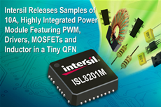
Intersil Releases Samples of 10A, Highly Integrated Power Module Featuring PWM, Drivers, MOSFETs and Inductor in a Tiny QFN Package
17:31Intersil Corporation a world leader in the design and manufacture of high-performance analog semiconductors, today announced the development of the ISL8201M, a highly integrated Power Conversion Module that saves space, reduces cost, and simplifies design.
The ISL8201M is a high efficiency, low noise, highly integrated DC/DC power solution in a thermally enhanced QFN package. Included in the package are the PWM controller, MOSFET drivers, power MOSFETs and inductor along with an optimized compensation circuit.
It simplifies power supply design as only input and output capacitors and a resistor is needed to implement a complete power solution. This small form factor saves considerable board space while the high integration reduces procurement and placement costs in various applications such as telecommunication, data communication, electronic data processing, wireless network systems, medical & instrumentation and distributed bus architecture based point of load applications. Also, an onboard input filter supports an ultra-low noise operation thus reducing EMI.
The ISL8201M achieves up to 93% efficiency and excellent thermal performance due to the QFN package that is designed to offer an optimum heat transfer through the PCB. A large copper plate under the package allows the ISL8201M to achieve a power density of approximately 200W/in3, roughly 4 times that of conventional open-frame modules thereby eliminating the need for heat sinks. Other features include internal soft-start, auto-recovery overcurrent protection, ENABLE pin option and pre-biased output start-up capability.
The high integration and performance of the ISL8201M is housed into a tiny 15mm x 15mm x 3.5mm QFN package
Pricing and Availability
The ISL8201M will soon be available for sampling in a 15-lead QFN package. For information, and pre-release samples, please contact Sarika Arora at (408) 546-3559 or by email at sarora01@intersil.com.
From: http://www.intersil.com
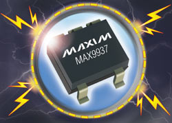
Tiny, Automotive-Grade Current-Sense Amplifier Has Reverse-Battery and Load-Dump Protection
17:27Maxim Integrated Products introduces the MAX9937, a tiny, high-side current-sense amplifier that uses external resistors to set the voltage gain for maximum design flexibility. The MAX9937 protects against accidental application of battery voltage in the reverse (wrong) direction and against inductive kickback transients and spikes (load dump) of -20V to +40V. These safeguards are a major concern in automotive electronic control units (ECUs), which are used to monitor currents in the modules that control electronic power steering, 4-wheel drive, and antilock braking systems; it even watches the fuse box so as to monitor problems.
The MAX9937 input common-mode range is 4V to 28V and is independent of the VCC supply voltage, which can operate at 2.7V to 5.5V. When VCC is 5V, the supply current is a low 20µA. When VCC is 0V, the input bias current at the sense resistor is only 1µA to minimize battery drain when the ECU is off.
Voltage gain is set by the ratio of two external resistors to their accuracy. Input offset voltage (VOS) is a low ±1.2mV (max).
The MAX9937 is available in tiny, 3mm x 3mm, 5-pin SC70 package that is lead- and halide-free, thereby RoHS-compliant. This amplifier is fully specified over the -40°C to +125°C automotive temperature range. Prices start at $0.58 (1000-up, FOB USA).
Maxim Integrated Products is a publicly traded company that designs, manufactures, and sells over $2 billion of high-performance semiconductor products annually. It was founded over 25 years ago with the mission to deliver innovative analog and mixed-signal engineering solutions that add value to its customers' products. To date, Maxim has developed over 5800 products serving the industrial, communications, consumer, and computing markets. For more information, go to www.maxim-ic.com.